S-1740 Overview
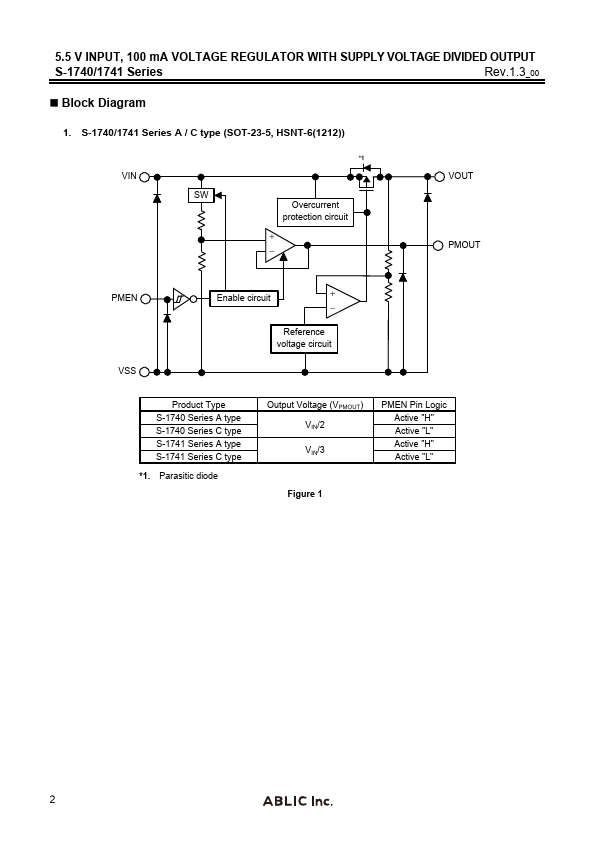
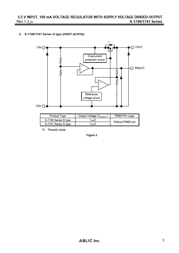
S-1740/1741 Series .ablic. © ABLIC Inc., 2016-2018 5.5 V INPUT, 100 mA VOLTAGE REGULATOR WITH SUPPLY VOLTAGE DIVIDED OUTPUT Rev.1.3_00 The S-1740/1741 Series, developed using CMOS technology, is a positive voltage regulator with the supply voltage divided output, which.
S-1740 Key Features
- Features
- Output voltage
- Input voltage
- Output voltage accuracy
- Dropout voltage
- Current consumption during operation
- Output current
- Input capacitor
- Output capacitor
- Built-in overcurrent protection circuit
S-1740 Applications
- Constant-voltage power supply and battery voltage monitoring support for battery-powered device
- Constant-voltage power supply for portable munication device, digital camera, and digital audio player
- Constant-voltage power supply for home electric appliance