Datasheet Summary
2'76;([[
®
$0,+- PLFURQ &026
- DWH $UUD
Description
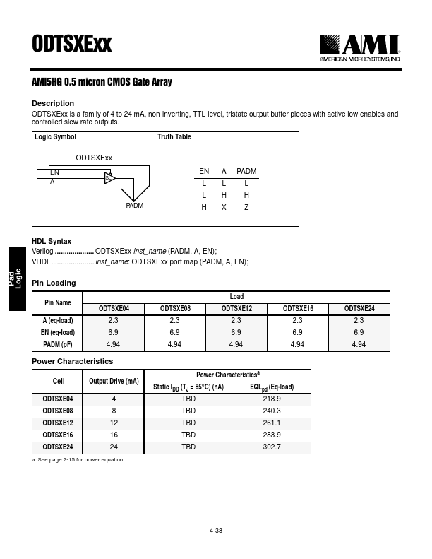
ODTSXExx is a family of 4 to 24 mA, non-inverting, TTL-level, tristate output buffer pieces with active low enables and controlled slew rate outputs.
Logic Symbol
Truth Table
ODTSXExx EN A SL
PADM
EN A PADM
LH H
HDL Syntax Verilog .................... ODTSXExx inst_name (PADM, A, EN); VHDL...................... inst_name: ODTSXExx port map (PADM, A, EN);
Pin Loading
Pin Name
A (eq-load) EN (eq-load) PADM (pF)
ODTSXE04 2.3 6.9 4.94
Power Characteristics
Cell Output Drive (mA)
ODTSXE04
ODTSXE08
ODTSXE16
ODTSXE24
24 a. See page 2-15 for power equation.
ODTSXE08 2.3 6.9 4.94
Load...