DESCRIPTION
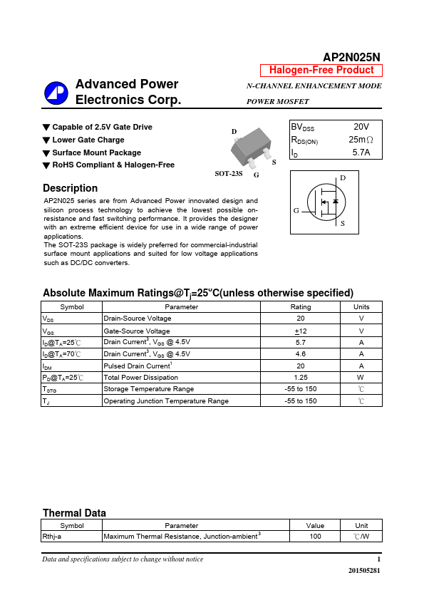
AP2N025 series are from Advanced Power innovated design and silicon process technology to achieve the lowest possible onresistance and fast switching performance. It provides the designer with an extreme efficient device for use in a wide range of power applications. S BVDSS RDS(ON) ID G 20V 25mΩ 5.7A D S ABSOLUTE MAXIMUM RATINGS
@Tj=25o.C(unless otherwise specified) Symbol Parameter Rating Units VDS Drain-Source Voltage 20 V VGS ID@TA=25℃ ID@TA=70℃ IDM PD@TA=25℃ TSTG TJ Gate-Source Voltage Drain Current3, VGS @ 4.5V Drain Current3, VGS @ 4.5V Pulsed Drain Current1 Total Power Dissipation Storage Temperature Range Operating Junction Temperature Range +12 5.7 4.6 20 1.25 -55 to 150 -55 to 150 V A A A W ℃ ℃ Thermal Data Symbol Parameter Rthj-a Maximum Thermal Resistance, Junction-ambient3 Data and specifications subject to change without notice Value 100 Unit ℃/W 1 201505281 AP2N025N ELECTRICAL CHARACTERISTICS
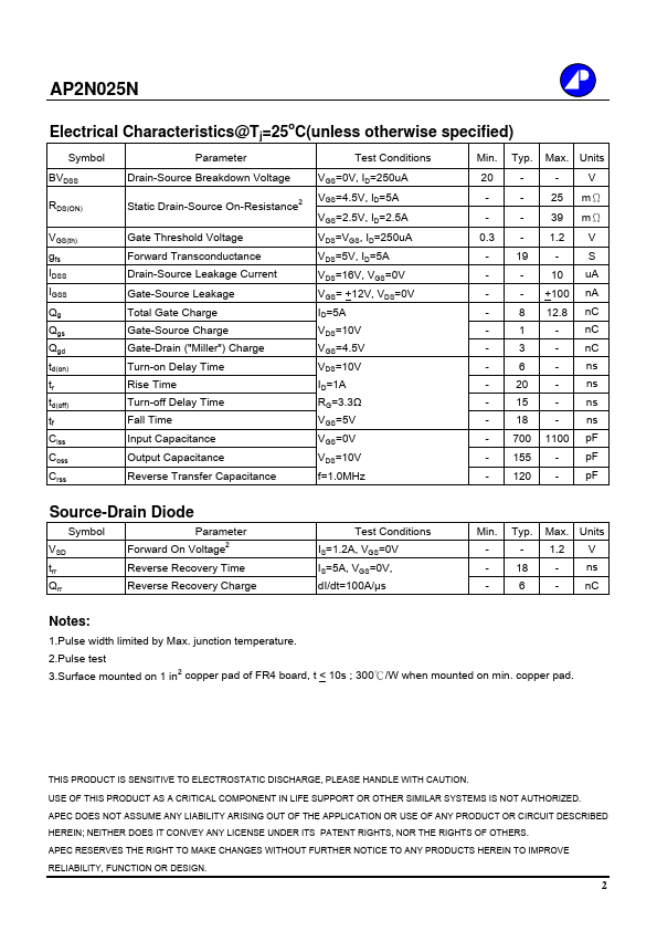
@Tj=25oC(unless otherwise specified) Symbol Parameter Test Conditions Min. Advanced Power Electronics