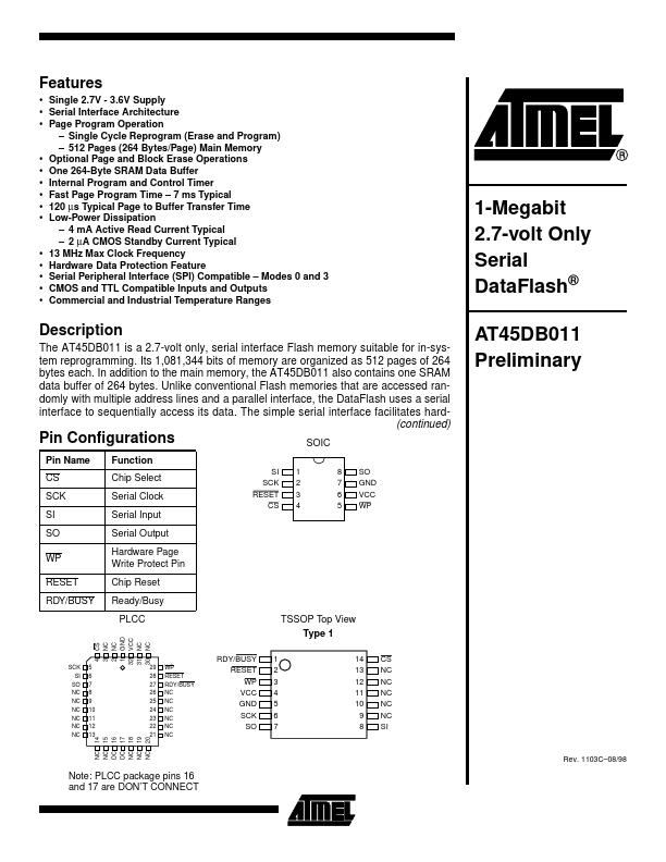
45DB011
Overview
...
| Part | 45DB011 |
|---|---|
| Description | AT45DB011 |
| Manufacturer | Atmel |
| Size | 149.41 KB |
...
| Part Number | Manufacturer | Description |
|---|---|---|
| HFDOM40B-xxxSx | Hanbit Electronics | 40Pin Flash Disk Module |
| HFDOM40P-xxxSx | Hanbit Electronics | 40Pin Flash Disk Module |
| FD777 | Fairchild Semiconductor | Ultra Fast Diodes |