AT16244F
Description
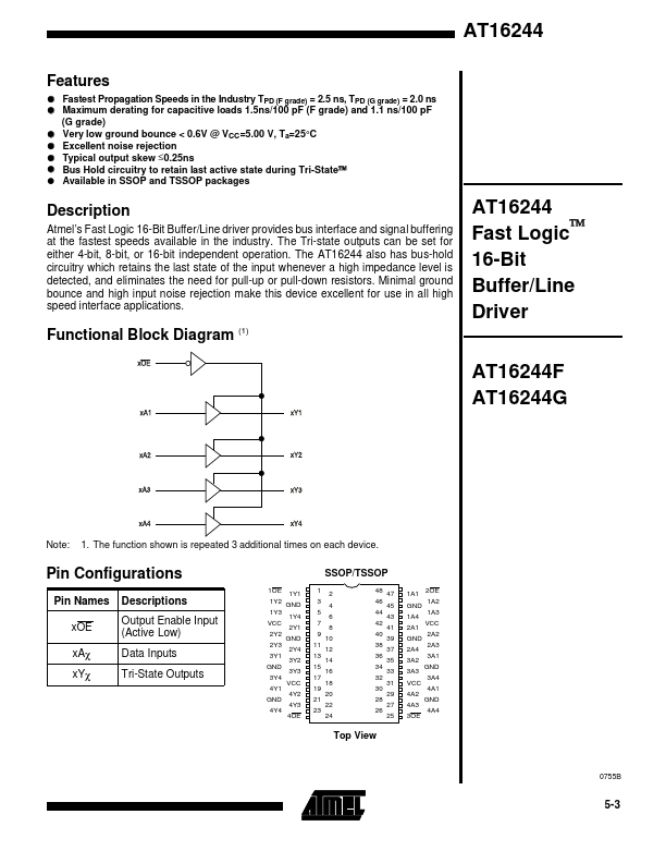
Atmel’s Fast Logic 16-Bit Buffer/Line driver provides bus interface and signal buffering at the fastest speeds available in the industry. The Tri-state outputs can be set for either 4-bit, 8-bit, or 16-bit independent operation.
Key Features
- Fastest Propagation Speeds in the Industry TPD (F grade) = 2.5 ns, TPD (G grade) = 2.0 ns Maximum derating for capacitive loads 1.5ns/100 pF (F grade) and 1.1 ns/100 pF (G grade) Very low ground bounce < 0.6V @ VCC =5.00 V, Ta=25°C Excellent noise rejection Typical output skew ≤0.25ns Bus Hold circuitry to retain last active state during Tri-State™ Available in SSOP and TSSOP packages