AT25F1024 Overview
Key Specifications
Package: SOIC
Mount Type: Surface Mount
Pins: 8
Max Voltage (typical range): 3.6 V
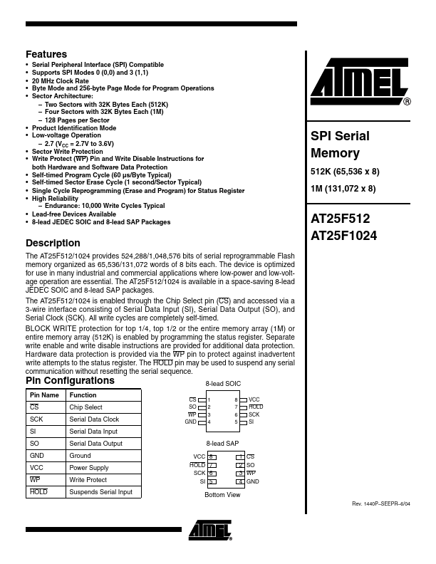
Description
The AT25F512/1024 provides 524,288/1,048,576 bits of serial reprogrammable Flash memory organized as 65,536/131,072 words of 8 bits each. The device is optimized for use in many industrial and commercial applications where low-power and low-voltage operation are essential.
Key Features
- Serial Peripheral Interface (SPI) Compatible
- 20 MHz Clock Rate
- Sector Architecture: – Two Sectors with 32K Bytes Each (512K) – Four Sectors with 32K Bytes Each (1M) – 128 Pages per Sector
- Product Identification Mode
- Low-voltage Operation – 2.7 (VCC = 2.7V to 3.6V)