AT25HP256 Overview
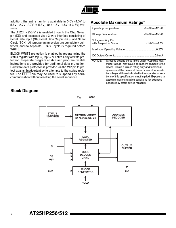
The device is optimized for use in many industrial and mercial applications where high-speed, low-power, and low-voltage operation are essential. The AT25HP256/512 is enabled through the Chip Select pin (CS) and accessed via a 3-wire interface consisting of Serial Data Input (SI), Serial Data Output (SO), and Serial Clock (SCK). All programming cycles are pletely selftimed, and no separate ERASE cycle is required...
AT25HP256 Key Features
- 5.0 (VCC = 4.5V to 5.5V)
- 2.7 (VCC = 2.7V to 5.5V)
- 1.8 (VCC = 1.8V to 3.6V) Block Write Protection
- Protect 1/4, 1/2, or Entire Array Write Protect (WP) Pin and Write Disable Instructions for Both Hardware and Software D
- Endurance: 100K Write Cycles
- Data Retention: > 40 Years
- ESD Protection: > 3000V 8-Pin PDIP, 8-Pin EIAJ SOIC, and 8-Pin Leadless Array Package
- SPI Serial EEPROMs
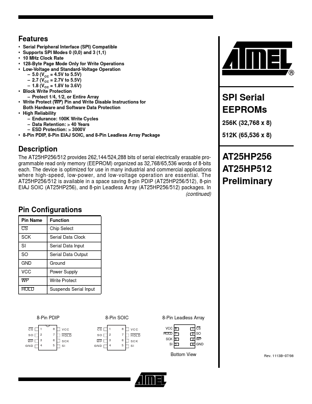
- Description