• Part: AT25P1024
  • Description: SPI Serial EEPROMs
  • Category: EEPROM
  • Manufacturer: Atmel
  • Size: 129.13 KB
Download AT25P1024 Datasheet PDF
Atmel
AT25P1024
AT25P1024 is SPI Serial EEPROMs manufactured by Atmel.
Features - - - - - Serial Peripheral Interface (SPI) patible Supports SPI Modes 0 (0,0) and 3 (1,1) 2.1 MHz Clock Rate 128-Byte Page Mode Only for Write Operations Low Voltage and Standard Voltage Operation - 5.0 (VCC = 4.5V to 5.5V) - 2.7 (VCC = 2.7V to 5.5V) - 1.8 (VCC = 1.8V to 3.6V) Block Write Protection - Protect 1/4, 1/2, or Entire Array Write Protect (WP) Pin and Write Disable Instructions for Both Hardware and Software Data Protection Self-Timed Write Cycle (5 ms Typical) High Reliability - Endurance: 100,000 Write Cycles - Data Retention: >40 Years - ESD Protection: >3000V 20-Pin JEDEC SOIC and 8-Pin Leadless Array Package - - - - SPI Serial EEPROMs 1M (131,072 x 8) - Description 
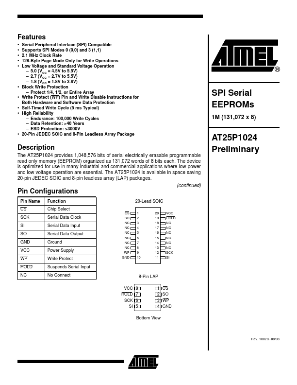
The AT25P1024 provides 1,048,576 bits of serial electrically erasable programmable read only memory (EEPROM) organized as 131,072 words of 8 bits each. The device is optimized for use in many industrial and mercial applications where low power and low voltage operation are essential. The AT25P1024 is available in space saving 20-pin JEDEC SOIC and 8-pin leadless array (LAP) packages. AT25P1024 Preliminary (continued) Pin Configurations Pin Name CS SCK SI SO GND VCC WP HOLD NC Function Chip Select Serial Data Clock Serial Data Input Serial Data Output Ground Power Supply Write Protect Suspends Serial Input No Connect VCC HOLD SCK SI 8 7 6 5 CS SO NC NC NC NC NC NC WP GND 1 2 3 4 5 6 7 8 9 10 20 19 18 17 16 15 14 13 12 11 VCC HOLD NC NC NC NC NC NC SCK SI 20-Lead SOIC 8-Pin LAP 1 2 3 4 CS SO WP GND Bottom View Rev. 1082C- 08/98 The AT25P1024 is enabled through the Chip Select pin (CS) and accessed via a 3-wire interface consisting of Serial Data Input (SI), Serial Data Output (SO), and Serial Clock (SCK). All programming cycles are pletely selftimed, and no separate ERASE cycle is required before WRITE. BLOCK WRITE protection is enabled by programming the status register with top ¼, top ½ or entire array of write protection. Separate program enable and program disable...