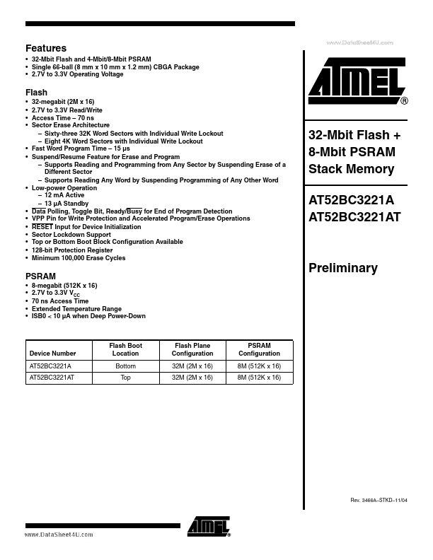
AT52BC3221A
Overview
- 32-Mbit Flash and 4-Mbit/8-Mbit PSRAM
- Single 66-ball (8 mm x 10 mm x 1.2 mm) CBGA Package
- 2.7V to 3.3V Operating Voltage Flash * * * * *
- 32-megabit (2M x 16) 2.7V to 3.3V Read/Write Access Time - 70 ns Sector Erase Architecture - Sixty-three 32K Word Sectors with Individual Write Lockout - Eight 4K Word Sectors with Individual Write Lockout Fast Word Program Time - 15 µs Suspend/Resume Feature for Erase and Program - Supports Reading and Programming from Any Sector by Suspending Erase of a Different Sector - Supports Reading Any Word by Suspending Programming of Any Other Word Low-power Operation - 12 mA Active - 13 µA Standby Data Polling, Toggle Bit, Ready/Busy for End of Program Detection VPP Pin for Write Protection and Accelerated Program/Erase Operations RESET Input for Device Initialization Sector Lockdown Support Top or Bottom Boot Block Configuration Available 128-bit Protection Register Minimum 100,000 Erase Cycles 32-Mbit Flash + 8-Mbit PSRAM Stack Memory AT52BC3221A AT52BC3221AT * * * * * * *
- PSRAM * * * *
- 8-megabit (512K x 16) 2.7V to 3.3V VCC 70 ns Access Time Extended Temperature Range ISB0 < 10 µA when Deep Power-Down Preliminary Device Number AT52BC3221A AT52BC3221AT Flash Boot Location Bottom Top Flash Plane Configuration 32M (2M x 16) 32M (2M x 16) PSRAM Configuration 8M (512K x 16) 8M (512K x 16) Rev. 3466A-STKD-11/04