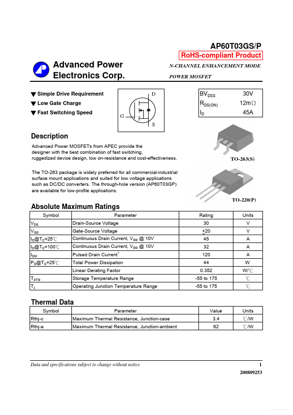
Download 60T03GP Datasheet PDF
Advanced Power Electronics Corp
60T03GP
60T03GP is N-CHANNEL ENHANCEMENT MODE POWER MOSFET manufactured by Advanced Power Electronics Corp.
Description Advanced Power MOSFETs from APEC provide the designer with the best bination of fast switching, ruggedized device design, low on-resistance and cost-effectiveness. The TO-263 package is widely preferred for all mercial-industrial surface mount applications and suited for low voltage applications such as DC/DC converters. The through-hole version (AP60T03GP) are available for low-profile applications. TO-263(S) TO-220(P) Absolute Maximum Ratings Symbol VDS VGS ID@TC=25℃ ID@TC=100℃ IDM PD@TC=25℃ TSTG TJ Parameter Drain-Source Voltage Gate-Source Voltage Continuous Drain Current, VGS @ 10V Continuous Drain Current, VGS @ 10V Pulsed Drain Current Rating 30 +20 45 32 120 44 0.352 -55 to 175 -55 to 175 Units V V A A A W W/℃ ℃ ℃ Total Power Dissipation Linear Derating Factor Storage Temperature Range Operating Junction Temperature Range Thermal Data Symbol Rthj-c Rthj-a Parameter Maximum Thermal Resistance, Junction-case Maximum Thermal Resistance, Junction-ambient Value 3.4 62 Units ℃/W ℃/W Data and specifications subject to change without notice 1 200809253 Free Datasheet http://../ AP60T03GS/P Electrical Characteristics@Tj=25o C(unless otherwise specified) Symbol BVDSS ΔBVDSS/ΔTj RDS(ON) VGS(th) gfs IDSS IGSS Qg Qgs Qgd td(on) tr td(off) tf Ciss Coss Crss Parameter Drain-Source Breakdown Voltage Static Drain-Source On-Resistance2 Test Conditions VGS=0V, ID=250u A Min. 30 1 Typ. 0.03 25 11.6 3.9 7 8.8 57.5 18.5 6.4 200 135 Max. Units 12 25 3 1 250 +100 19 V V/℃ mΩ mΩ V S u A u A n A n C n C n C ns ns ns ns p F p F p F Breakdown Voltage Temperature Coefficient Reference to 25℃, ID=1m A VGS=10V, ID=20A VGS=4.5V, ID=15A VDS=VGS, ID=250u A Gate Threshold Voltage Forward Transconductance VDS=10V, ID=10A VDS=30V, VGS=0V o Drain-Source Leakage Current Gate-Source Leakage Total Gate Charge Drain-Source Leakage Current (T j=175 C) VDS=24V ,VGS=0V VGS= +20V ID=20A VDS=24V VGS=4.5V VDS=15V ID=20A RG=3.3Ω,VGS=10V RD=0.75Ω VGS=0V VDS=25V f=1.0MHz Gate-Source...