AP15T15GM-HF
AP15T15GM-HF is N-CHANNEL ENHANCEMENT MODE POWER MOSFET manufactured by Advanced Power Electronics Corp.
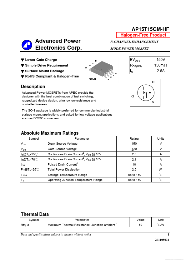
Description
Advanced Power MOSFETs from APEC provide the designer with the best bination of fast switching, ruggedized device design, ultra low on-resistance and cost-effectiveness. The SO-8 package is widely preferred for mercial-industrial surface mount applications and suited for low voltage applications such as DC/DC converters.
Absolute Maximum Ratings
Symbol VDS VGS ID@TA=25℃ ID@TA=70℃ IDM PD@TA=25℃ TSTG TJ Parameter Drain-Source Voltage Gate-Source Voltage Continuous Drain Current , VGS @ 10V Continuous Drain Current , VGS @ 10V Pulsed Drain Current
1 3 3
Rating 150 +20 2.6 2.1 10 2.5 -55 to 150 -55 to 150
Units V V A A A W ℃ ℃
Total Power Dissipation Storage Temperature Range Operating Junction Temperature Range
Thermal Data
Symbol Rthj-a Parameter Maximum Thermal Resistance, Junction-ambient
Value 50
Unit ℃/W 1 201105031
Data and specifications subject to change without notice
Free Datasheet http://../
Electrical Characteristics@Tj=25o C(unless otherwise specified)
Symbol BVDSS RDS(ON) VGS(th) gfs IDSS IGSS Qg Qgs Qgd td(on) tr td(off) tf Ciss Coss Crss Rg Parameter Drain-Source Breakdown Voltage Static Drain-Source On-Resistance
Test Conditions VGS=0V, ID=250u A VGS=10V, ID=2A VGS=4.5V, ID=1A VDS=VGS, ID=250u A VDS=10V, ID=2A VDS=120V, VGS=0V VGS=+20V, VDS=0V ID=2A VDS=75V VGS=10V VDS=75V ID=1A RG=3.3Ω VGS=10V VGS=0V VDS=15V f=1.0MHz f=1.0MHz
Min. 150 1
- Typ. 4 22.5 3.5 7.5 8 5.5 25 10 115 75 1.2
Max. Units 150 250 3 1 +100 36 2.4 V mΩ mΩ V S u A n A n C n C n C ns ns ns ns p F p F p F Ω
Gate Threshold Voltage Forward Transconductance Drain-Source Leakage Current Gate-Source Leakage Total Gate Charge Gate-Source Charge Gate-Drain ("Miller") Charge Turn-on Delay Time Rise Time Turn-off Delay Time Fall Time Input Capacitance Output Capacitance Reverse Transfer Capacitance Gate Resistance
1050 1680
Source-Drain Diode
Symbol VSD trr Qrr Parameter Forward On Voltage
Test Conditions IS=1.9A, VGS=0V IS=8A, VGS=0V, d I/dt=100A/µs
Mi...