AP15T20GI-HF
AP15T20GI-HF is N-CHANNEL ENHANCEMENT MODE POWER MOSFET manufactured by Advanced Power Electronics Corp.
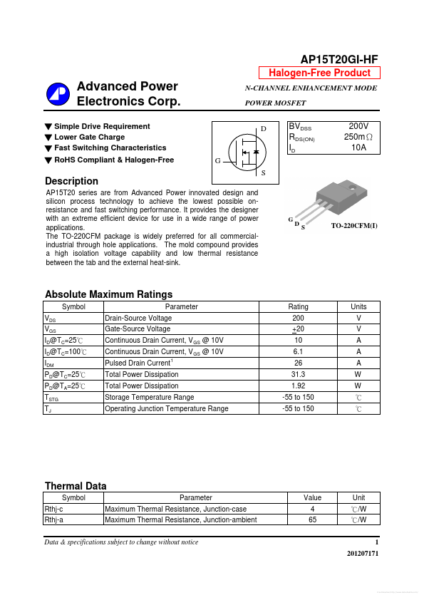
Description
AP15T20 series are from Advanced Power innovated design and silicon process technology to achieve the lowest possible onresistance and fast switching performance. It provides the designer with an extreme efficient device for use in a wide range of power applications. The TO-220CFM package is widely preferred for all mercialindustrial through hole applications. The mold pound provides a high isolation voltage capability and low thermal resistance between the tab and the external heat-sink.
TO-220CFM(I)
Absolute Maximum Ratings
Symbol VDS VGS ID@TC=25℃ ID@TC=100℃ IDM PD@TC=25℃ PD@TA=25℃ TSTG TJ Parameter Drain-Source Voltage Gate-Source Voltage Continuous Drain Current, V GS @ 10V Continuous Drain Current, V GS @ 10V Pulsed Drain Current
Rating 200 +20 10 6.1 26 31.3 1.92 -55 to 150 -55 to 150
Units V V A A A W W ℃ ℃
Total Power Dissipation Total Power Dissipation Storage Temperature Range Operating Junction Temperature Range
Thermal Data
Symbol Rthj-c Rthj-a Parameter Maximum Thermal Resistance, Junction-case Maximum Thermal Resistance, Junction-ambient Value 4 65 Unit ℃/W ℃/W 1 201207171
Data & specifications subject to change without notice
Free Datasheet http://../
Electrical Characteristics@Tj=25 C(unless otherwise specified)
Symbol BVDSS RDS(ON) VGS(th) gfs IDSS IGSS Qg Qgs Qgd td(on) tr td(off) tf Ciss Coss Crss Rg Parameter Drain-Source Breakdown Voltage Static Drain-Source On-Resistance 2 Gate Threshold Voltage Forward Transconductance Drain-Source Leakage Current Gate-Source Leakage Total Gate Charge Gate-Source Charge Gate-Drain ("Miller") Charge Turn-on Delay Time Rise Time Turn-off Delay Time Fall Time Input Capacitance Output Capacitance Reverse Transfer Capacitance Gate Resistance Test Conditions VGS=0V, ID=250u A VGS=10V, ID=5A VGS=4.5V, ID=3A VDS=VGS, ID=250u A VDS=10V, ID=5A VDS=160V, VGS=0V VGS= +20V, VDS=0V ID=5A VDS=160V VGS=10V VDD=100V ID=5A RG=3.3Ω VGS=10V VGS=0V VDS=25V f=1.0MHz f=1.0MHz Min. 200 1...