AP2306CGN-HF
AP2306CGN-HF is N-CHANNEL ENHANCEMENT MODE POWER MOSFET manufactured by Advanced Power Electronics Corp.
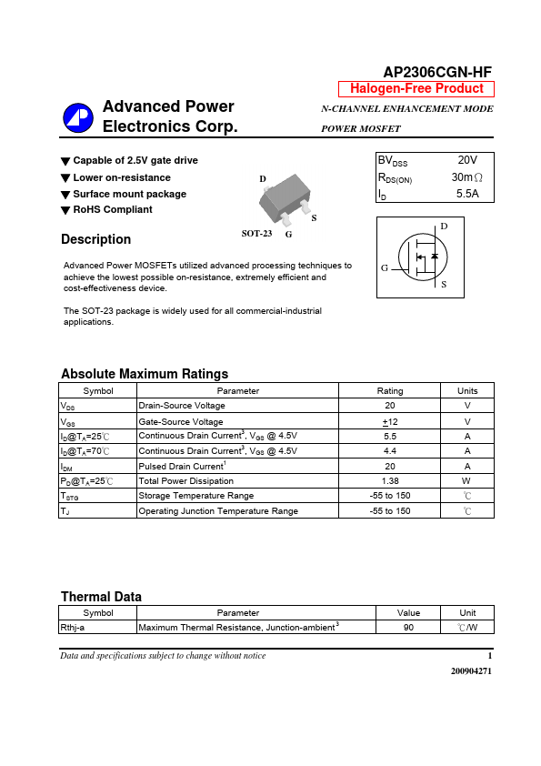
Description
Advanced Power MOSFETs utilized advanced processing techniques to achieve the lowest possible on-resistance, extremely efficient and cost-effectiveness device. The SOT-23 package is widely used for all mercial-industrial applications.
Absolute Maximum Ratings
Symbol VDS VGS ID@TA=25℃ ID@TA=70℃ IDM PD@TA=25℃ TSTG TJ Parameter Drain-Source Voltage Gate-Source Voltage Continuous Drain Current , VGS @ 4.5V Continuous Drain Current , VGS @ 4.5V Pulsed Drain Current
1 3 3
Rating 20 +12 5.5 4.4 20 1.38 -55 to 150 -55 to 150
Units V V A A A W ℃ ℃
Total Power Dissipation Storage Temperature Range Operating Junction Temperature Range
Thermal Data
Symbol Rthj-a Parameter Maximum Thermal Resistance, Junction-ambient
Value 90
Unit ℃/W 1 200904271
Data and specifications subject to change without notice
Electrical Characteristics@Tj=25o C(unless otherwise specified)
Symbol BVDSS RDS(ON) VGS(th) gfs IDSS IGSS Qg Qgs Qgd td(on) tr td(off) tf Ciss Coss Crss Parameter Drain-Source Breakdown Voltage Static Drain-Source On-Resistance2 Test Conditions VGS=0V, ID=250u A VGS=4.5V, ID=5 VGS=2.5V, ID=2.5A Gate Threshold Voltage Forward Transconductance Drain-Source Leakage Current Gate-Source Leakage Total Gate Charge2 Gate-Source Charge Gate-Drain ("Miller") Charge Turn-on Delay Time Rise Time Turn-off Delay Time Fall Time Input Capacitance Output Capacitance Reverse Transfer Capacitance
Min. 20 0.3
- Typ. 18 11 1.2 4.4 6 11 25 4 610 90 80
Max. Units 30 45 1.2 1 +100 18 980 V mΩ mΩ V S u A n A n C n C n C ns ns ns ns p F p F p F
VDS=VGS, ID=250u A VDS=5V, ID=5A VDS=20V, VGS=0V VGS= +12V, VDS=0V ID=5A VDS=16V VGS=4.5V VDS=10V ID=1A RG=3.3Ω,VGS=10V RD=10Ω VGS=0V VDS=20V f=1.0MHz
Source-Drain Diode
Symbol VSD trr Qrr Parameter Forward On Voltage
2 2
Test Conditions IS=1.2A, VGS=0V IS=5A, VGS=0V, d I/dt=100A/µs
Min.
- Typ. 20 13
Max. Units 1.2 V ns n C
Reverse Recovery Time
Reverse Recovery Charge
Notes:
1.Pulse width limited by Max. junction...