AP40T03GI
AP40T03GI is N-CHANNEL ENHANCEMENT MODE POWER MOSFET manufactured by Advanced Power Electronics Corp.
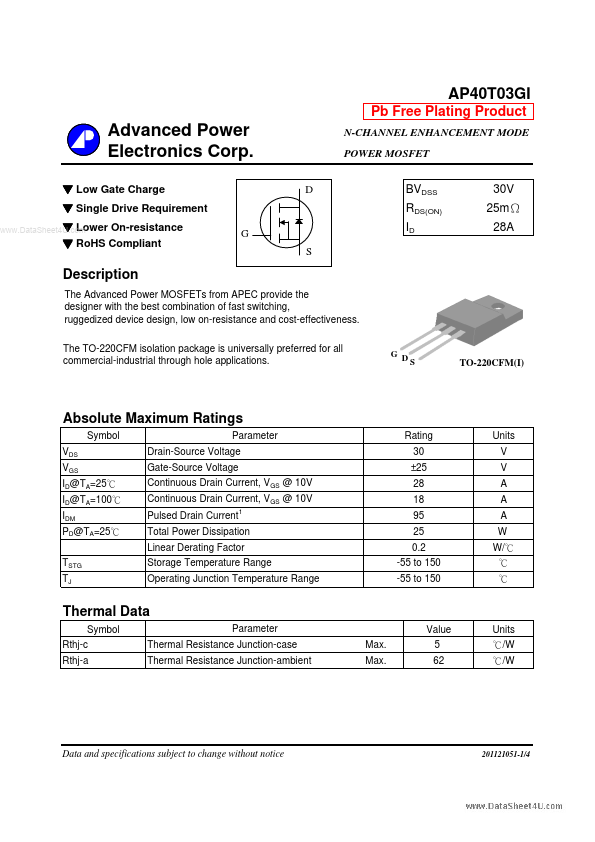
Description
The Advanced Power MOSFETs from APEC provide the designer with the best bination of fast switching, ruggedized device design, low on-resistance and cost-effectiveness. The TO-220CFM TO-252 package isolation is universally package preferred is universally for all preferred mercialfor all industrial surface mount mercial-industrial through applications hole applications. and suited for low voltage
TO-220CFM(I)
Absolute Maximum Ratings
Symbol VDS VGS ID@TA=25℃ ID@TA=100℃ IDM PD@TA=25℃ TSTG TJ Parameter Drain-Source Voltage Gate-Source Voltage Continuous Drain Current, VGS @ 10V Continuous Drain Current, VGS @ 10V Pulsed Drain Current
Rating 30 ±25 28 18 95 25 0.2 -55 to 150 -55 to 150
Units V V A A A W W/℃ ℃ ℃
Total Power Dissipation Linear Derating Factor Storage Temperature Range Operating Junction Temperature Range
Thermal Data
Symbol Rthj-c Rthj-a Parameter Thermal Resistance Junction-case Thermal Resistance Junction-ambient Max. Max. Value 5 62 Units ℃/W ℃/W
Data and specifications subject to change without notice
201121051-1/4
Electrical Characteristics@Tj=25o C(unless otherwise specified)
Symbol BVDSS
ΔBVDSS/ΔTj
Parameter Drain-Source Breakdown Voltage
Test Conditions VGS=0V, ID=250u A
Min. 30 1
- Typ. 0.02 16 9 2 6 7 56 16 5 610 160 117 1.5
Max. Units 25 45 3 1 25 ±100 15 980 2.3 V V/℃ mΩ mΩ V S u A u A n A n C n C n C ns ns ns ns p F p F p F Ω
Breakdown Voltage Temperature Coefficient Reference to 25℃, ID=1m A
RDS(ON)
..
Static Drain-Source On-Resistance
VGS=10V, ID=18A VGS=4.5V, ID=14A
VGS(th) gfs IDSS IGSS Qg Qgs Qgd td(on) tr td(off) tf Ciss Coss Crss Rg
Gate Threshold Voltage Forward Transconductance
Drain-Source Leakage Current (T j=25 C) Drain-Source Leakage Current (T j=150 C) o o
VDS=VGS, ID=250u A VDS=10V, ID=18A VDS=30V, VGS=0V VDS=24V ,VGS=0V VGS= ±25V ID=18A VDS=25V VGS=4.5V VDS=15V ID=18A RG=3.3Ω,VGS=10V RD=0.83Ω VGS=0V VDS=25V f=1.0MHz f=1.0MHz
Gate-Source Leakage Total Gate Charge
Gate-Source Charge...