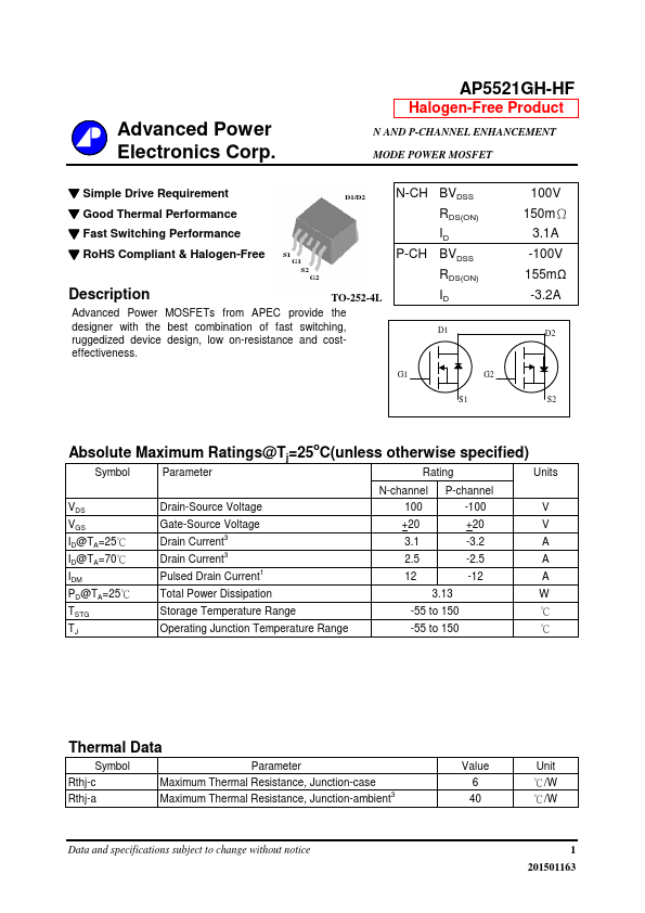
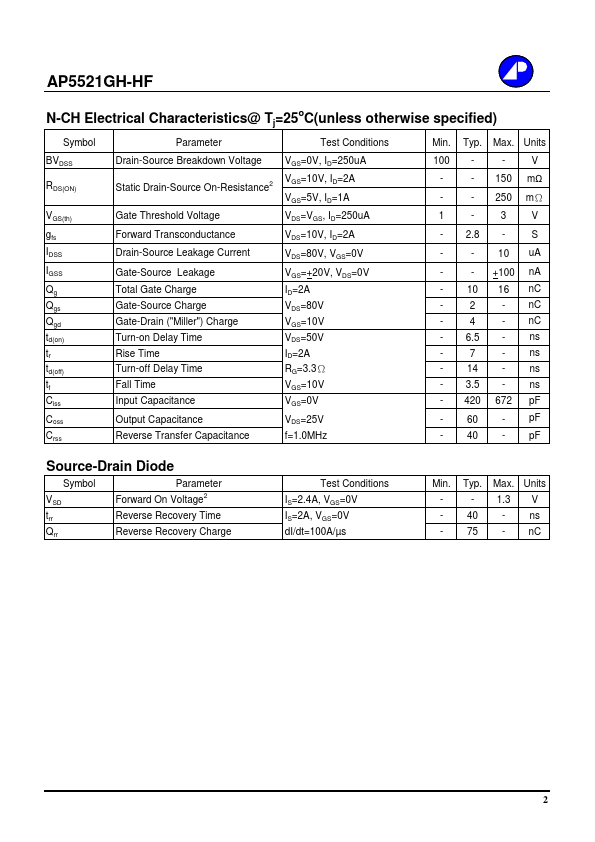
Datasheet Details
| Part number | AP5521GH-HF |
|---|---|
| Manufacturer | Advanced Power Electronics Corp |
| File Size | 83.46 KB |
| Description | N AND P-CHANNEL ENHANCEMENT MODE POWER MOSFET |
| Download | AP5521GH-HF Download (PDF) |
|
|
|
Overview: Advanced Power Electronics Corp. AP5521GH-HF Halogen-Free Product N AND P-CHANNEL ENHANCEMENT MODE POWER MOSFET ▼ Simple Drive Requirement ▼ Good Thermal Performance D1/D2 ▼ Fast Switching Performance ▼ RoHS Compliant &.
| Part number | AP5521GH-HF |
|---|---|
| Manufacturer | Advanced Power Electronics Corp |
| File Size | 83.46 KB |
| Description | N AND P-CHANNEL ENHANCEMENT MODE POWER MOSFET |
| Download | AP5521GH-HF Download (PDF) |
|
|
|
TO-252-4L Advanced Power MOSFETs from APEC provide the designer with the best combination of fast switching, ruggedized device design, low on-resistance and costeffectiveness.
N-CH P-CH BVDSS RDS(ON) ID BVDSS RDS(ON) ID D1 G1 G2 S1 100V 150mΩ 3.1A -100V 155mΩ -3.2A D2 S2 Absolute Maximum Ratings@Tj=25oC(unless otherwise specified) Symbol Parameter Rating Units N-channel P-channel VDS VGS ID@TA=25℃ ID@TA=70℃ IDM PD@TA=25℃ TSTG TJ Drain-Source Voltage Gate-Source Voltage Drain Current3 Drain Current3 Pulsed Drain Current1 Total Power Dissipation Storage Temperature Range Operating Junction Temperature Range 100 -100 +20 +20 3.1 -3.2 2.5 -2.5 12 -12 3.13 -55 to 150 -55 to 150 V V A A A W ℃ ℃ Thermal Data Symbol Parameter Rthj-c Rthj-a Maximum Thermal Resistance, Junction-case Maximum Thermal Resistance, Junction-ambient3 Data and specifications subject to change without notice Value 6 40 Unit ℃/W ℃/W 1 201501163 AP5521GH-HF N-CH Electrical Characteristics@ Tj=25oC(unless otherwise specified) Symbol BVDSS RDS(ON) VGS(th) gfs IDSS IGSS Qg Qgs Qgd td(on) tr td(off) tf Ciss Coss Crss Parameter Test Conditions Drain-Source Breakdown Voltage Static Drain-Source On-Resistance2 VGS=0V, ID=250uA VGS=10V, ID=2A VGS=5V, ID=1A Gate Threshold Voltage VDS=VGS, ID=250uA Forward Transconductance Drain-Source Leakage Current VDS=10V, ID=2A VDS=80V, VGS=0V Gate-Source Leakage Total Gate Charge Gate-Source Charge Gate-Drain ("Miller") Charge Turn-on Delay Time Rise Time Turn-off Delay Time Fall Time Input Capacitance Output Capacitance Reverse Transfer Capacitance VGS=+20V, VDS=0V ID=2A VDS=80V VGS=10V VDS=50V ID=2A RG=3.3Ω VGS=10V VGS=0V VDS=25V f=1.0MHz Min.
Typ.
| Brand Logo | Part Number | Description | Manufacturer |
|---|---|---|---|
![]() |
AP5521GM-HF | N- and P-Channel 100V MOSFET | VBsemi |
| Part Number | Description |
|---|---|
| AP5521GM-HF | N AND P-CHANNEL ENHANCEMENT MODE POWER MOSFET |
| AP5523GM-HF | N AND P-CHANNEL ENHANCEMENT MODE POWER MOSFET |
| AP55T06GI-HF | N-CHANNEL ENHANCEMENT MODE POWER MOSFET |
| AP55T10GH-HF | N-CHANNEL ENHANCEMENT MODE POWER MOSFET |
| AP55T10GH-HF-3 | N-CHANNEL ENHANCEMENT MODE POWER MOSFET |
| AP55T10GI-HF | N-CHANNEL ENHANCEMENT MODE POWER MOSFET |
| AP55T10GP-HF | N-CHANNEL ENHANCEMENT MODE POWER MOSFET |
| AP55T10GP-HF-3 | N-CHANNEL ENHANCEMENT MODE POWER MOSFET |
| AP55T10GS-HF | N-CHANNEL ENHANCEMENT MODE POWER MOSFET |
| AP50G60SW | N-CHANNEL INSULATED GATE BIPOLAR TRANSISTOR |