AP9962AGJ-HF
AP9962AGJ-HF is N-CHANNEL ENHANCEMENT MODE POWER MOSFET manufactured by Advanced Power Electronics Corp.
- Part of the AP9962AGH-HF comparator family.
- Part of the AP9962AGH-HF comparator family.
Description
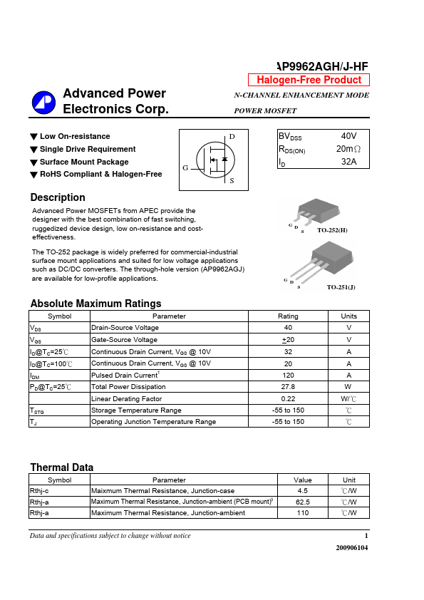
Advanced Power MOSFETs from APEC provide the designer with the best bination of fast switching, ruggedized device design, low on-resistance and costeffectiveness. The TO-252 package is widely preferred for mercial-industrial surface mount applications and suited for low voltage applications such as DC/DC converters. The through-hole version (AP9962AGJ) are available for low-profile applications.
TO-252(H)
TO-251(J)
Absolute Maximum Ratings
Symbol VDS VGS ID@TC=25℃ ID@TC=100℃ IDM PD@TC=25℃ TSTG TJ Parameter Drain-Source Voltage Gate-Source Voltage Continuous Drain Current, VGS @ 10V Continuous Drain Current, VGS @ 10V Pulsed Drain Current
Rating 40 +20 32 20 120 27.8 0.22 -55 to 150 -55 to 150
Units V V A A A W W/ ℃ ℃ ℃
Total Power Dissipation Linear Derating Factor Storage Temperature Range Operating Junction Temperature Range
Thermal Data
Symbol Rthj-c Rthj-a Rthj-a Parameter Maixmum Thermal Resistance, Junction-case
Maximum Thermal Resistance, Junction-ambient (PCB mount)3
Value 4.5 62.5 110
Unit ℃/W ℃/W ℃/W 1 200906104
Maximum Thermal Resistance, Junction-ambient
Data and specifications subject to change without notice
AP9962AGH/J-HF
Electrical Characteristics@Tj=25o C(unless otherwise specified)
Symbol BVDSS RDS(ON) VGS(th) gfs IDSS IGSS Qg Qgs Qgd td(on) tr td(off) tf Ciss Coss Crss Parameter Drain-Source Breakdown Voltage Static Drain-Source On-Resistance
Test Conditions VGS=0V, ID=250u A VGS=10V, ID=20A VGS=4.5V, ID=16A VDS=VGS, ID=250u A VDS=10V, ID=20A VDS=40V, VGS=0V o
Min. 40 1
- Typ. 40 12 2.7 7.8 7 46 20 6 820 95 90
Max. Units 20 30 3 10 250 +100 20 1800 V mΩ mΩ V S u A u A n A n C n C n C ns ns ns ns p F p F p F
Gate Threshold Voltage Forward Transconductance Drain-Source Leakage Current Gate-Source Leakage Total Gate Charge
Drain-Source Leakage Current (T j=125 C) VDS=32V ,VGS=0V
VGS= +20V, VDS=0V ID=20A VDS=32V VGS=4.5V VDS=20V ID=20A RG=3.3Ω,VGS=10V RD=1.0Ω VGS=0V VDS=25V f=1.0MHz
Gate-Source Charge Gate-Drain...