Datasheet4U Logo Datasheet4U.com

STRA6169 - Universal-Input/5W Flyback Switching Regulator

Download the STRA6169 datasheet PDF. This datasheet also covers the STR-A6169 variant, as both devices belong to the same universal-input/5w flyback switching regulator family and are provided as variant models within a single manufacturer datasheet.

General Description

and applications information is provided in Application Note 28102.20, Series STRA6100 Flyback Switching Regulators.

The products described herein are manufactured in Japan by Sanken Electric Co., Ltd.

for sale by Allegro MicroSystems, Inc.

Key Features

  • Rugged 800 V Avalanche-Rated MOSFET Simplified Surge Absorption No VDSS Derating Required.
  • 19.2 Ω rDS(on).
  • Two Operational Modes by Automatic Switching: PRC Mode for Normal Operation Burst Mode for Stand-By Operation or Light Loads.
  • Built-In Leading Edge Blanking.
  • Low Start-Up Current Start-Up Circuit Disabled in Operation.
  • Low Operating Current (1.5 mA typ).
  • Automatic Burst Stand-By (intermittent operation) Input Power.

📥 Download Datasheet

Note: The manufacturer provides a single datasheet file (STR-A6169-AllegroMicrosystems.pdf) that lists specifications for multiple related part numbers.

Full PDF Text Transcription (Reference)

The following content is an automatically extracted verbatim text from the original manufacturer datasheet and is provided for reference purposes only.

View original datasheet text
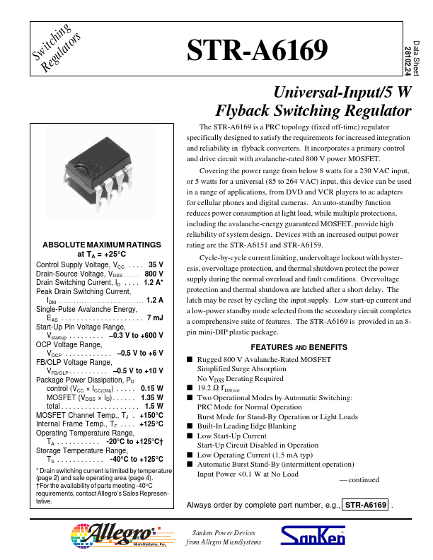
Data Sheet 28102.24 SwRitecghuinlagtors ABSOLUTE MAXIMUM RATINGS at TA = +25°C Control Supply Voltage, VCC . . . . 35 V Drain-Source Voltage, VDSS . . . . . . 800 V Drain Switching Current, ID . . . . 1.2 A* Peak Drain Switching Current, IDM . . . . . . . . . . . . . . . . . . . . . . . . . . . . . . . . . 1.2 A Single-Pulse Avalanche Energy, EAS . . . . . . . . . . . . . . . . . . . . . 7 mJ Start-Up Pin Voltage Range, Vstartup . . . . . . . . . –0.3 V to +600 V OCP Voltage Range, VOCP . . . . . . . . . . . . –0.5 V to +6 V FB/OLP Voltage Range, VFB/OLP . . . . . . . . . . –0.5 V to +10 V Package Power Dissipation, PD control (VCC × ICC(ON)) . . . . . 0.15 W MOSFET (VDSS × ID) . . . . . . 1.35 W total . . . . . . . . . . . . . . . . . . . . 1.5 W MOSFET Channel Temp., TJ .