Datasheet4U Logo Datasheet4U.com

AS8C401800 - 3.3V Synchronous SRAMs

Download the AS8C401800 datasheet PDF. This datasheet also covers the AS8C403600 variant, as both devices belong to the same 3.3v synchronous srams family and are provided as variant models within a single manufacturer datasheet.

General Description

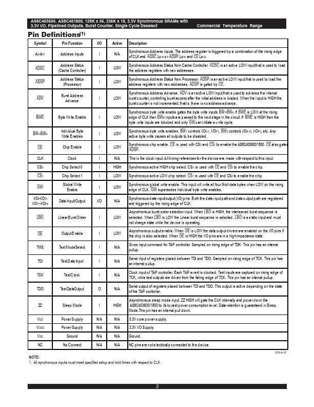
TheAS8C403600/1800 are high- speed SRAMs organized as 128K x 36/256K x 18.

The AS8C403600/401800 SRAMs contain write, data, address and control registers.

Key Features

  • 128K x 36, 256K x 18 memory configurations Supports high system speed: Commercial:.
  • 150MHz 3.8ns clock access time LBO input selects interleaved or linear burst mode Self-timed write cycle with global write control ( GW l ( ), byte write enable (BWE), and byte writes ( BWx) 3.3V core power supply Power down controlled by ZZ input 3.3V I/O Optional - Boundary Scan JTAG Interface (IEEE 1149.1 compliant) Packaged in a JEDEC Standard 100-pin plastic thin quad flatpack (TQFP).

📥 Download Datasheet

Note: The manufacturer provides a single datasheet file (AS8C403600-AllianceSemiconductor.pdf) that lists specifications for multiple related part numbers.

Datasheet Details

Part number AS8C401800
Manufacturer Alliance Semiconductor
File Size 1.08 MB
Description 3.3V Synchronous SRAMs
Datasheet download datasheet AS8C401800 Datasheet

Full PDF Text Transcription (Reference)

The following content is an automatically extracted verbatim text from the original manufacturer datasheet and is provided for reference purposes only.

View original datasheet text
128K x 36, 256K x 18 3.3V Synchronous SRAMs 3.3V I/O, Pipelined Outputs Burst Counter, Single Cycle Deselect ◆ ◆ AS8C403600 AS8C401800 Features 128K x 36, 256K x 18 memory configurations Supports high system speed: Commercial: – 150MHz 3.8ns clock access time LBO input selects interleaved or linear burst mode Self-timed write cycle with global write control ( GW l ( ), byte write enable (BWE), and byte writes ( BWx) 3.3V core power supply Power down controlled by ZZ input 3.3V I/O Optional - Boundary Scan JTAG Interface (IEEE 1149.1 compliant) Packaged in a JEDEC Standard 100-pin plastic thin quad flatpack (TQFP). Description ◆ ◆ ◆ ◆ ◆ ◆ ◆ TheAS8C403600/1800 are high- speed SRAMs organized as 128K x 36/256K x 18.