AO4601
Description
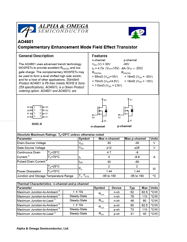
The AO4601 uses advanced trench technology MOSFETs to provide excellent RDS(ON) and low gate charge. The plementary MOSFETs may be used to form a level shifted high side switch, and for a host of other applications.
The AO4601 uses advanced trench technology MOSFETs to provide excellent RDS(ON) and low gate charge. The plementary MOSFETs may be used to form a level shifted high side switch, and for a host of other applications.
| Part Number | Manufacturer | Description |
|---|---|---|
| AO4604 | Kexin Semiconductor | Complementary Trench MOSFET |