AO4603 Datasheet (PDF) Download
Alpha & Omega Semiconductors
AO4603

Description

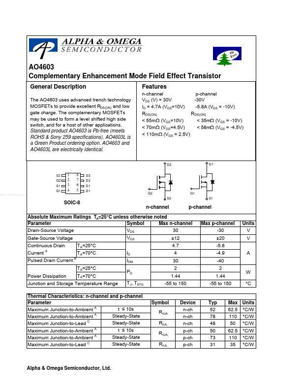
The AO4603 uses advanced trench technology MOSFETs to provide excellent RDS(ON) and low gate charge. The complementary MOSFETs may be used to form a level shifted high side switch, and for a host of other applications.

Key Features

  • 0 RDS(ON) limited TJ(Max)=150°C TA=25°C 10µs Power (W) 20 TJ(Max)=150°C TA=25°C
  • 0 ID (Amps) 1ms 15 100µs 0.1s 10ms 10
  • 0 1s 10s DC 0.1 0.1 1 VDS (Volts) Figure 9: Maximum Forward Biased Safe Operating Area (Note E) 10 100 5 0 0.001
  • 1 1 10 100 1000 Pulse Width (s) Figure 10: Single Pulse Power Rating Junction-toAmbient (Note E) 10 Zθ JA Normalized Transient Thermal Resistance D=Ton/T TJ,PK=TA+PDM.ZθJA.RθJA RθJA=90°C/W In descending order D=0.5, 0.3, 0.1, 0.05, 0.02, 0.01, single pulse 1
  • 1 PD Ton Single Pulse T
  • 01 0.00001
  • 1 1 10 100 1000 Pulse Width (s) Figure 11: Normalized Maximum Transient Thermal Impedance Alpha & Omega Semiconductor, Ltd. AO4603 p-channel MOSFET Electrical Characteristics (T J=25°C unless otherwise noted) Symbol Parameter Conditions ID=-250µA, VGS=0V VDS=-24V, VGS=0V TJ=55°C VDS=0V, VGS=±20V VDS=VGS ID=-250µA VGS=-10V, VDS=-5V VGS=-10V, ID=-5A RDS(ON) gFS VSD IS Static Drain-Source On-Resistance VGS=-4.5V, ID=-5A Forward Transconductance VDS=-5V, ID=-10A -0.75 -1 -4.2 920 VGS=0V, VDS=-15V, f=1MHz VGS=0V, VDS=0V, f=1MHz 190 122 3.6 2.4 VGS=-10V, VDS=-15V, ID=-7.5A 4.5 9.3 7.6 VGS=-10V, VDS=-15V, RL=2Ω, RGEN=3Ω IF=-7.5A, dI/dt=100A/µs 5.2 21.6 8 20 8.8 Diode Forward Voltage IS=-1A,VGS=0V Maximum Body-Diode Continuous Current TJ=125°C -1.2 40 29 40 39 63 38 -1.8 Min -30 -1 -5 ±100 -2.2 Typ Max Units V µA nA V A mΩ mΩ S V A pF pF pF Ω nC nC nC ns ns ns ns ns nC