AOB29S50L
AOB29S50L is Power Transistor manufactured by Alpha & Omega Semiconductors.
AOT29S50L/AOB29S50L/AOTF29S50L/AOTF29S50
500V 29A a MOS TM Power Transistor
General Description
Product Summary
The AOT29S50L & AOB29S50L & AOTF29S50L & AOTF29S50 have been fabricated using the advanced a MOSTM high voltage process that is designed to deliver high levels of performance and robustness in switching applications. By providing low RDS(on), Qg and EOSS along with guaranteed avalanche capability these parts can be adopted quickly into new and existing offline power supply designs.
VDS @ Tj,max IDM RDS(ON),max Qg,typ Eoss @ 400V
100% UIS Tested 100% Rg Tested
600V 120A 0.15W 26.6n C 6.3m J
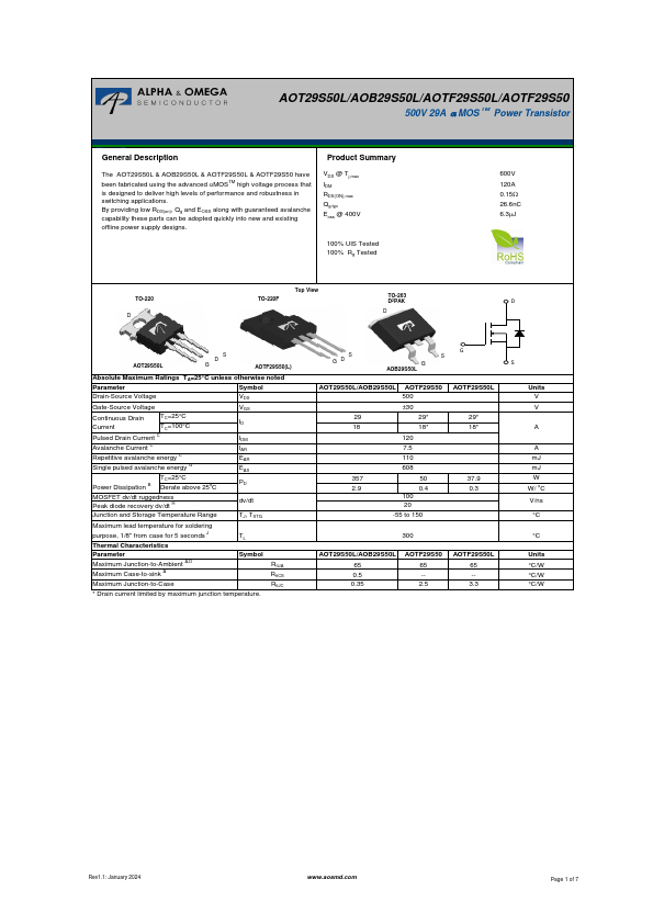
Top View
TO-220
TO-220F
TO-263
D2PAK
AOT29S50L
AOTF29S50(L)...