Datasheet Details
| Part number | AOI508 |
|---|---|
| Manufacturer | Alpha & Omega Semiconductors |
| File Size | 302.94 KB |
| Description | 30V N-Channel MOSFET |
| Download | AOI508 Download (PDF) |
|
|
| Part number | AOI508 |
|---|---|
| Manufacturer | Alpha & Omega Semiconductors |
| File Size | 302.94 KB |
| Description | 30V N-Channel MOSFET |
| Download | AOI508 Download (PDF) |
|
|
|
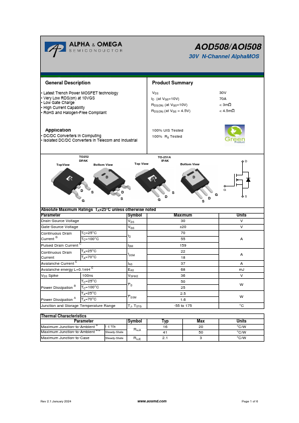
• Latest Trench Power MOSFET technology • Very Low RDS(on) at 10VGS • Low Gate Charge • High Current Capability • RoHS and Halogen-Free Compliant Product Summary VDS ID (at VGS=10V) RDS(ON) (at VGS=10V) RDS(ON) (at VGS = 4.5V) 30V 70A < 3mW < 4.5mW Application • DC/DC Converters in Computing • Isolated DC/DC Converters in Telecom and Industrial 100% UIS Tested 100% Rg Tested TO252 TO-251A DPAK IPAK D TopView Bottom View Top View Bottom View D D DS G DG S S D G Absolute Maximum Ratings TA=25°C unless otherwise noted Parameter Symbol Drain-Source Voltage VDS Gate-Source Voltage VGS Continuous Drain Current G TC=25°C TC=100°C ID Pulsed Drain Current C IDM Continuous Drain Current TA=25°C TA=70°C IDSM Avalanche Current C IAS Avalanche energy L=0.1mH C EAS VDS Spike 100ns VSPIKE TC=25°C Power Dissipation B TC=100°C PD TA=25°C Power Dissipation A TA=70°C PDSM Junction and Storage Temperature Range TJ, TSTG Maximum 30 ±20 70 55 159 22 18 37 68 36 50 25 2.5 1.6 -55 to 175 G G D S Thermal Characteristics Parameter Symbol Typ Maximum Junction-to-Ambient A t ≤ 10s Maximum Junction-to-Ambient A D Steady-State RqJA 16 41 Maximum Junction-to-Case Steady-State RqJC 2.1 Max 20 50 3 S Units V V A A A mJ V W W °C Units °C/W °C/W °C/W Rev 2.1:January 2024 www.aosmd.com Page 1 of 6 AOD508/AOI508 Electrical Characteristics (TJ=25°C unless otherwise noted) Symbol Parameter Conditions Min Typ Max Units STATIC PARAMETERS BVDSS Drain-Source Breakdown Voltage ID=250mA, VGS=0V 30 V IDSS Zero Gate Voltage Drain Current VDS=30V, VGS=0V TJ=55°C 1 mA 5 IGSS Gate-Body leakage current VDS=0V, VGS= ±20V 100 nA VGS(th) Gate Threshold Voltage VDS=VGS,ID=250mA 1.2 1.8 2.2 V RDS(ON) Static Drain-Source On-Resistance VGS=10V, ID=20A TJ=125°C 2.4 3 mW 3.5 4.4 VGS=4.5V, ID=20A 3.3 4.5 mW gFS Forward Transconductance VDS=5V, ID=20A 105 S VSD Diode
AOD508/AOI508 30V N-Channel AlphaMOS General.
| Brand Logo | Part Number | Description | Manufacturer |
|---|---|---|---|
| AOI508 | N-Channel MOSFET | INCHANGE |
| Part Number | Description |
|---|---|
| AOI510 | 30V N-Channel MOSFET |
| AOI514 | 30V N-Channel MOSFET |
| AOI516 | 30V N-Channel MOSFET |
| AOI518 | 30V N-Channel MOSFET |
| AOI538 | 30V N-Channel MOSFET |
| AOI5N40 | 4.2A N-Channel MOSFET |
| AOI11S60 | Power Transistor |
| AOI1N60 | 1.3A N-Channel MOSFET |
| AOI206 | 30V N-Channel MOSFET |
| AOI21357 | P-Channel MOSFET |