AON6278 Overview
Key Specifications
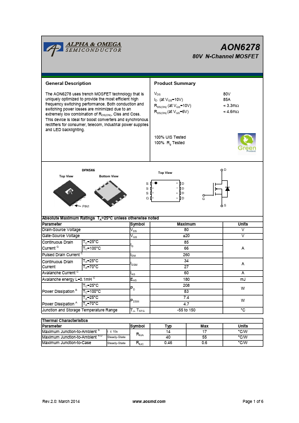
Package: DFN
Mount Type: Surface Mount
Pins: 8
Height: 1 mm
Description
Product Summary The AON6278 uses trench MOSFET technology that is uniquely optimized to provide the most efficient high frequency switching performance. Both conduction and switching power losses are minimized due to an extremely low combination of RDS(ON), Ciss and Coss.