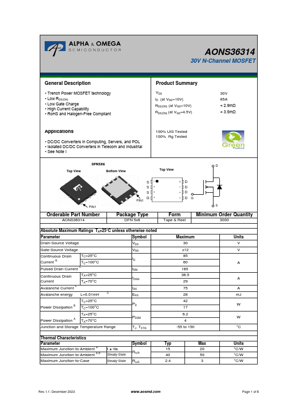
AONS36314
Electrical Characteristics (TJ=25°C unless otherwise noted)
Symbol Parameter
Conditions
Min Typ Max Units
STATIC PARAMETERS
BVDSS Drain-Source Breakdown Voltage
IDSS Zero Gate Voltage Drain Current
ID=250μA, VGS=0V
VDS=30V, VGS=0V
IGSS
VGS(th)
RDS(ON)
gFS
VSD
IS
Gate-Body leakage current
Gate Threshold Voltage
VDS=0V, VGS=±12V
VDS=VGS, ID=250mA
VGS=10V, ID=20A
Static Drain-Source On-Resistance
Forward Transconductance
VGS=4.5V, ID=20A
VDS=5V, ID=20A
Diode Forward Voltage
IS=1A, VGS=0V
Maximum Body-Diode Continuous Current
TJ=55°C
TJ=125°C
30
1.1
V
1 μA
5
±100 nA
1.5 1.9 V
2.4 2.9 mΩ
3.4 4.1
2.8 3.5 mΩ
100 S
0.7 1 V
50 A
DYNAMIC PARAMETERS
Ciss Input Capacitance
Coss Output Capacitance
Crss Reverse Transfer Capacitance
Rg Gate resistance
VGS=0V, VDS=15V, f=1MHz
f=1MHz
1890
395
55
1.2 2.3
3.6
pF
pF
pF
Ω
SWITCHING PARAMETERS
Qg(10V) Total Gate Charge
Qg(4.5V) Total Gate Charge
Qgs Gate Source Charge
VGS=10V, VDS=15V, ID=20A
Qgd Gate Drain Charge
tD(on)
Turn-On DelayTime
tr
tD(off)
Turn-On Rise Time
Turn-Off DelayTime
VGS=10V, VDS=15V, RL=0.75W,
RGEN=3W
tf Turn-Off Fall Time
trr Body Diode Reverse Recovery Time IF=20A, di/dt=500A/ms
Qrr Body Diode Reverse Recovery Charge IF=20A, di/dt=500A/ms
27.5 40 nC
11.5 18 nC
6 nC
2.5 nC
7.5 ns
3.5 ns
30 ns
4 ns
12 ns
21 nC
A. The value of RqJA is measured with the device mounted on 1in 2 FR-4 board with 2oz. Copper, in a still air environment with T A =25°C. The Power
dissipation PDSM is based on R qJA t≤ 10s and the maximum allowed junction temperature of 150 °C. The value in any given application depends on
the user's specific board design.
B. The power dissipation PD is based on TJ(MAX)=150°C, using junction-to-case thermal resistance, and is more useful in setting the upper dissipation
limit for cases where additional heatsinking is used.
C. Single pulse width limited by junction temperature T J(MAX)=150°C.
D. The RqJA is the sum of the thermal impedance from junction to case R qJC and case to ambient.
E. The static characteristics in Figures 1 to 6 are obtained using <300 ms pulses, duty cycle 0.5% max.
F. These curves are based on the junction-to-case thermal impedance which is measured with the device mounted to a large heatsin k, assuming a
maximum junction temperature of TJ(MAX)=150°C. The SOA curve provides a single pulse rating.
G. The maximum current rating is package limited.
H. These tests are performed with the device mounted on 1 in 2 FR-4 board with 2oz. Copper, in a still air environment with T A=25°C.
I. For application requiring slow >1ms turn -on/turn-off, please consult AOS FAE for proper product selection.
APPLICATIONS OR USE AS CRITICAL COMPONENTS IN LIFE SUPPORT DEVICES OR SYSTEMS ARE NOT AUTHORIZED. AOS DOES NOT
ASSUME ANY LIABILITY ARISING OUT OF SUCH APPLICATIONS OR USES OF ITS PRODUCTS. AOS RESERVES THE RIGHT TO IMPROVE
PRODUCT DESIGN,FUNCTIONS AND RELIABILITY WITHOUT NOTICE.
Rev.1.0: August 2018
www.aosmd.com
Page 2 of 6