Datasheet Details
| Part number | AOSD21313C |
|---|---|
| Manufacturer | Alpha & Omega Semiconductors |
| File Size | 329.86 KB |
| Description | 30V Dual P-Channel MOSFET |
| Datasheet | AOSD21313C-AlphaOmegaSemiconductors.pdf |
|
|
Overview: AOSD21313C 30V Dual P-Channel MOSFET General.
| Part number | AOSD21313C |
|---|---|
| Manufacturer | Alpha & Omega Semiconductors |
| File Size | 329.86 KB |
| Description | 30V Dual P-Channel MOSFET |
| Datasheet | AOSD21313C-AlphaOmegaSemiconductors.pdf |
|
|
|
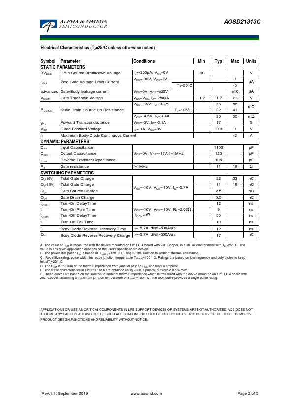
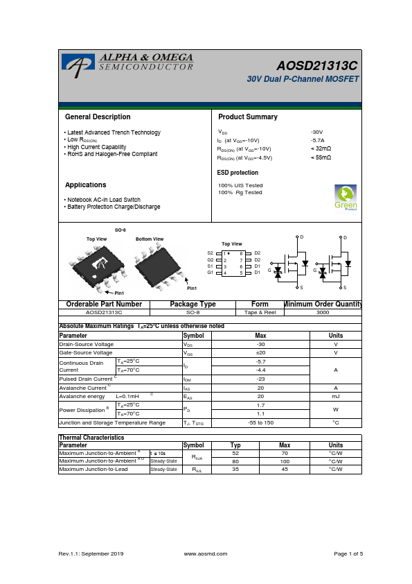
• Latest Advanced Trench Technology • Low RDS(ON) • High Current Capability • RoHS and Halogen-Free Compliant Applications • Notebook AC-in Load Switch • Battery Protection Charge/Discharge Product Summary VDS ID (at VGS=-10V) RDS(ON) (at VGS=-10V) RDS(ON) (at VGS=-4.5V) ESD protection 100% UIS Tested 100% Rg Tested -30V -5.7A < 32mΩ < 55mΩ Top View SO-8 Bottom View Top View S2 1 8 G2 2 7 S1 3 6 G1 4 5 D2 D2 D1 D1 G D D G Pin1 Orderable Part Number AOSD21313C Pin1 Package Type SO-8 S S Form Minimum Order Quantity Tape & Reel 3000 Absolute Maximum Ratings TA=25°C unless otherwise noted Parameter Symbol Drain-Source Voltage VDS Gate-Source Voltage VGS Continuous Drain Current TA=25°C TA=70°C ID Pulsed Drain Current C IDM Avalanche Current C IAS Avalanche energy L=0.1mH C EAS Power Dissipation B TA=25°C TA=70°C PD Junction and Storage Temperature Range TJ, TSTG Max -30 ±20 -5.7 -4.4 -23 20 20 1.7 1.1 -55 to 150 Units V V A A mJ W °C Thermal Characteristics Parameter Symbol Typ Maximum Junction-to-Ambient A t ≤ 10s Maximum Junction-to-Ambient A D Steady-State RqJA 52 80 Maximum Junction-to-Lead Steady-State RqJL 35 Max 70 100 45 Units °C/W °C/W °C/W Rev.1.1: September 2019 www.aosmd.com Page 1 of 5 AOSD21313C Electrical Characteristics (TJ=25°C unless otherwise noted) Symbol Parameter Conditions Min STATIC PARAMETERS BVDSS Drain-Source Breakdown Voltage ID=-250mA, VGS=0V -30 IDSS Zero Gate Voltage Drain Current • Latest VDS=-30V, VGS=0V TJ=55°C advanced Gate-Body leakage current VDS=0V, VGS=±20V VGS(th) Gate Threshold Voltage VDS=VGS, ID=-250mA -1.2 VGS=-10V, ID=-5.7A RDS(ON) Static Drain-Source On-Resistance TJ=125°C VGS=-4.5V, ID=-4.4A gFS Forward Transconductance VDS=-5V, ID=-5.7A VSD Diode Forward Voltage IS=-1A, VGS=0V IS Maximum Body-Diode Continuous Current DYNAMIC PARAMETERS Ciss Input Capacitance Coss Outp
| Part Number | Description |
|---|---|
| AOSD21311C | 30V Dual P-Channel MOSFET |
| AOSD21307 | 30V Dual P-Channel MOSFET |
| AOSD26313C | 30V Complementary MOSFET |
| AOSD32334C | 30V Dual N-Channel MOSFET |
| AOSD62666E | 60V Dual N-Channel MOSFET |
| AOSN32128 | 20V N-Channel MOSFET |
| AOSP21307 | 30V P-Channel MOSFET |
| AOSP21311C | 30V P-Channel MOSFET |
| AOSP21313C | 30V P-Channel MOSFET |
| AOSP21321 | 30V P-Channel MOSFET |