Datasheet4U Logo Datasheet4U.com

AOT2142L Datasheet N-Channel MOSFET

Manufacturer: Alpha & Omega Semiconductors

General Description

• Trench Power MV MOSFET technology • Low RDS(ON) • Low Gate Charge • Optimized for fast-switching applications Product Summary VDS ID (at VGS=10V) RDS(ON) (at VGS=10V) RDS(ON) (at VGS=4.5V) Applications • Synchronous Rectification in DC/DC and AC/DC Converters • Isolated DC/DC Converters in Telecom and Industrial 100% UIS Tested 100% Rg Tested
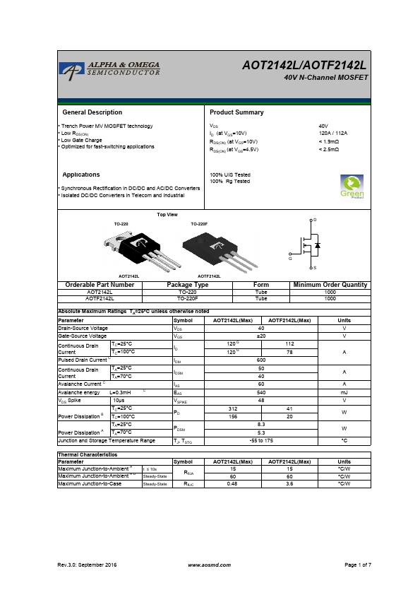
 TO-220 Top View TO-220F 40V 120A / 112A < 1.9mΩ < 2.5mΩ D AOT2142L Orderable Part Number AOT2142L AOTF2142L AOTF2142L Package Type TO-220 TO-220F Form Tube Tube G S Minimum Order Quantity 1000 1000 Absolute Maximum Ratings TA=25°C unless otherwise noted Parameter Symbol AOT2142L(Max) AOTF2142L(Max) Drain-Source Voltage VDS 40 Gate-Source Voltage VGS Continuous Drain Current TC=25°C TC=100°C ID Pulsed Drain Current C IDM Continuous Drain Current TA=25°C TA=70°C IDSM Avalanche Current C IAS Avalanche energy L=0.3mH C EAS ±20 120 G 112 120 G 78 600 50 40 60 540 VDS Spike Power Dissipation B 10µs TC=25°C TC=100°C VSPIKE PD 48 312 41 156 20 TA=25°C Power Dissipation A TA=70°C PDSM 8.3 5.3 Junction and Storage Temperature Range TJ, TSTG -55 to 175 Units V V A A A mJ V W W °C Thermal Characteristics Parameter Maximum Junction-to-Ambient A Maximum Junction-to-Ambient A D Maximum Junction-to-Case t ≤ 10s Steady-State Steady-State Symbol RθJA RθJC AOT2142L(Max) 15 60 0.48 AOTF2142L(Max) 15 60 3.6 Units °C/W °C/W °C/W Rev.3.0: September 2016 www.aosmd.com Page 1 of 7 AOT2142L/AOTF2142L Electrical Characteristics (TJ=25°C unless otherwise noted) Symbol Parameter Conditions Min STATIC PARAMETERS BVDSS Drain-Source Breakdown Voltage ID=250µA, VGS=0V 40 IDSS Zero Gate Voltage Drain Current VDS=40V, VGS=0V TJ=55°C IGSS Gate-Body leakage current VDS=0V, VGS=±20V VGS(th) Gate Threshold Voltage VDS=VGS, ID=250µA 1.3 VGS=10V, ID=20A RDS(ON) Static Drain-Source On-Resistance TJ=125°C VGS=4.5V, ID=2

Overview

AOT2142L/AOTF2142L 40V N-Channel MOSFET General.