Description
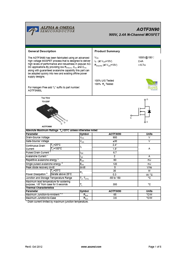
Product Summary The AOTF3N90 has been fabricated using an advanced high voltage MOSFET process that is designed to deliver high levels of performance and robustness in popular ACDC applications.By providing low RDS(on), Ciss and Crss along with guaranteed avalanche capability this part can be adopted quickly into new and existing offline power supply designs. For Halogen Free add "L" suffix to part number: AOTF3N90L VDS ID (at VGS=10V) RDS(ON) (at VGS=10V) 100% UIS Tested 100% Rg Tested Top View TO-220F 1000V@150℃ 2.4A < 6.7Ω D AOTF3N90 S D G Parameter Symbol Drain-Source Voltage VDS Gate-Source Voltage VGS Continuous Drain TC=25°C Current TC=100°C Pulsed Drain Current C Avalanche Current C Repetitive avalanche energy C Single pulsed avalanche energy G Peak diode recovery dv/dt ID IDM IAR EAR EAS dv/dt TC=25°C Power Dissipation B Derate above 25oC PD Junction and Storage Temperature Range Maximum lead temperature for soldering purpose, 1/8" from case for 5 seconds TJ, TSTG TL Parameter Symbol Maximum Junction-to-Ambient A,D RθJA Maximum Junction-to-Case RθJC * Drain current limited by maximum junction temperature.