AOUS66416
AOUS66416 is N-Channel MOSFET manufactured by Alpha & Omega Semiconductors.
Description
- Trench Power MOSFET
- Alpha SGTTM technology
- Low RDS(ON)
- Excellent QG x RDS(ON) Product (FOM)
- Ro HS and Halogen-Free pliant
Product Summary
VDS ID (at VGS=10V) RDS(ON) (at VGS=10V) RDS(ON) (at VGS=4.5V)
Applications
- High frequency switching and synchronous rectification
- Synchronous rectification MOSFET for Server Power, ATX Power, Adaptor, Tele power
100% UIS Tested 100% Rg Tested
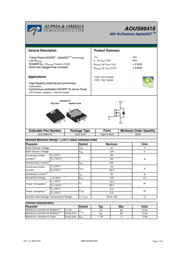
Ultra SO-8TM
Top View
Bottom View
40V 69A < 3.3mΩ < 5.0mΩ
Orderable Part Number
Package Type
Ultra SO8
Form
Tape & Reel
Minimum Order Quantity
Absolute Maximum Ratings TA=25°C unless otherwise noted
Parameter
Symbol
Drain-Source Voltage
Gate-Source Voltage
Continuous Drain TC=25°C
Current G
TC=100°C
Pulsed Drain Current C
Continuous Drain Current
Avalanche Current C
TA=25°C...