Datasheet Details
| Part number | AOWF14N50 |
|---|---|
| Manufacturer | Alpha & Omega Semiconductors |
| File Size | 285.37 KB |
| Description | 14A N-Channel MOSFET |
| Download | AOWF14N50 Download (PDF) |
|
|
Overview: AOW14N50/AOWF14N50 500V, 14A N-Channel MOSFET General.
Download the AOWF14N50 datasheet PDF. This datasheet also includes the AOW14N50 variant, as both parts are published together in a single manufacturer document.
| Part number | AOWF14N50 |
|---|---|
| Manufacturer | Alpha & Omega Semiconductors |
| File Size | 285.37 KB |
| Description | 14A N-Channel MOSFET |
| Download | AOWF14N50 Download (PDF) |
|
|
|
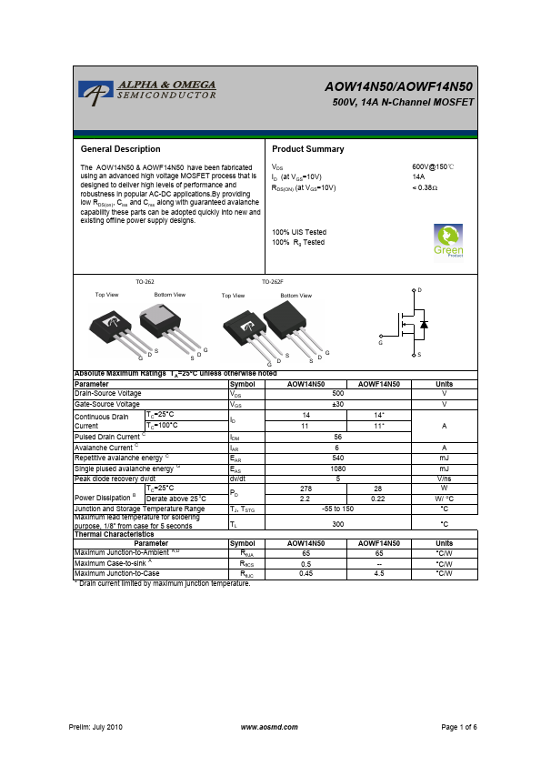
Product Summary The AOW14N50 & AOWF14N50 have been fabricated using an advanced high voltage MOSFET process that is designed to deliver high levels of performance and robustness in popular AC-DC applications.By providing low RDS(on), Ciss and Crss along with guaranteed avalanche capability these parts can be adopted quickly into new and existing offline power supply designs.
VDS ID (at VGS=10V) RDS(ON) (at VGS=10V) 100% UIS Tested 100% Rg Tested Top View TO-262 Bottom View Top View TO-262F Bottom View 600V@150℃ 14A < 0.38Ω D G G DS G SD S GD G SD Absolute Maximum Ratings TA=25°C unless otherwise noted Parameter Symbol AOW14N50 AOWF14N50 Drain-Source Voltage VDS 500 Gate-Source Voltage VGS ±30 Continuous Drain TC=25°C Current TC=100°C Pulsed Drain Current C Avalanche Current C Repetitive avalanche energy C Single plused avalanche energy G Peak diode recovery dv/dt ID IDM IAR EAR EAS dv/dt 14 11 56 6 540 1080 5 14* 11* TC=25°C Power Dissipation B Derate above 25oC PD 278 28 2.2 0.22 Junction and Storage Temperature Range Maximum lead temperature for soldering purpose, 1/8" from case for 5 seconds Thermal Characteristics TJ, TSTG TL -55 to 150 300 Parameter Maximum Junction-to-Ambient A,D Maximum Case-to-sink A Symbol RθJA RθCS AOW14N50 65 0.5 AOWF14N50 65 -- Maximum Junction-to-Case RθJC * Drain current limited by maximum junction temperature.
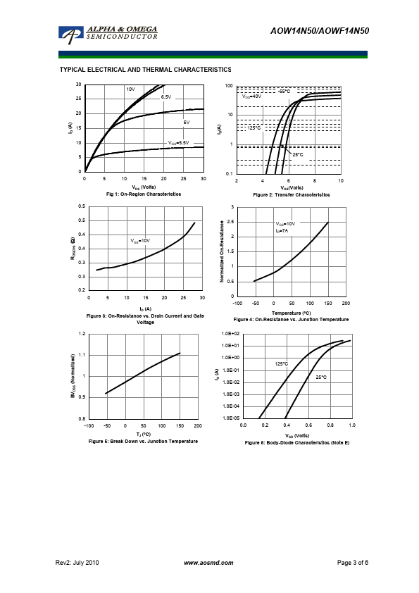
0.45 4.5 S Units V V A A mJ mJ V/ns W W/ oC °C °C Units °C/W °C/W °C/W Prelim: July 2010 www.aosmd.com Page 1 of 6 AOW14N50/AOWF14N50 Electrical Characteristics (TJ=25°C unless otherwise noted) Symbol Parameter Conditions Min Typ Max Units STATIC PARAMETERS BVDSS Drain-Source Breakdown Voltage ID=250µA, VGS=0V, TJ=25°C ID=250µA, VGS=0V, TJ=150°C 500 600 V BVDSS /∆TJ Breakdown Voltage Temperature Coefficient ID=250µA, VGS=0V 0.5 V/ oC IDSS IGSS VGS(th) RDS(ON) gFS VSD IS ISM Zero Gate Voltage Dra
| Part Number | Description |
|---|---|
| AOWF10N60 | 10A N-Channel MOSFET |
| AOWF10N65 | 10A N-Channel MOSFET |
| AOWF10T60 | 10A N-Channel MOSFET |
| AOWF11C60 | 11A N-Channel MOSFET |
| AOWF11S60 | Power Transistor |
| AOWF11S65 | Power Transistor |
| AOWF125A60 | N-Channel Power Transistor |
| AOWF12N50 | 12A N-Channel MOSFET |
| AOWF12N60 | 12A N-Channel MOSFET |
| AOWF12N65 | 12A N-Channel MOSFET |