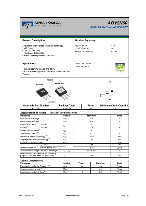
Electrical Characteristics (TJ=25°C unless otherwise noted)
Symbol
Parameter
Conditions
Min Typ Max Units
STATIC PARAMETERS
BVDSS Drain-Source Breakdown Voltage
ID=250µA, VGS=0V, TJ=25°C
ID=250µA, VGS=0V, TJ=150°C
BVDSS
/∆TJ
Zero Gate Voltage Drain Current
ID=250µA, VGS=0V
IDSS
Zero Gate Voltage Drain Current
VDS=600V, VGS=0V
VDS=480V, TJ=125°C
IGSS
Gate-Body leakage current
VDS=0V, VGS=±30V
VGS(th) Gate Threshold Voltage
VDS=5V, ID=250µA
RDS(ON) Static Drain-Source On-Resistance
VGS=10V, ID=1A
gFS
Forward Transconductance
VSD
Diode Forward Voltage
VDS=40V, ID=1A
IS=1A,VGS=0V
IS
Maximum Body-Diode Continuous Current
ISM
Maximum Body-Diode Pulsed Current C
DYNAMIC PARAMETERS
Ciss
Input Capacitance
Coss
Output Capacitance
VGS=0V, VDS=25V, f=1MHz
Crss
Reverse Transfer Capacitance
Rg
Gate resistance
f=1MHz
SWITCHING PARAMETERS
Qg
Total Gate Charge
Qgs
Gate Source Charge
VGS=10V, VDS=480V, ID=2A
Qgd
Gate Drain Charge
tD(on)
tr
tD(off)
Turn-On DelayTime
Turn-On Rise Time
Turn-Off DelayTime
VGS=10V, VDS=300V, ID=2A,
RG=25Ω
tf
Turn-Off Fall Time
trr
Body Diode Reverse Recovery Time IF=2A,dI/dt=100A/µs,VDS=100V
Qrr
Body Diode Reverse Recovery Charge IF=2A,dI/dt=100A/µs,VDS=100V
600
700
V
0.7
V/ oC
1
µA
10
±100 nΑ
3.4
4
4.5
V
3.9 4.7
Ω
2.8
S
0.79 1
V
2
A
6
A
295
pF
30
pF
2.3
pF
3.2
Ω
6.5 11 nC
1.5
nC
1.8
nC
16
ns
11
ns
28
ns
14
ns
268
ns
1.6
µC
A. The value of R θJA is measured with the device in a still air environment with T A =25°C.
B. The power dissipation PD is based on TJ(MAX)=150°C in a TO252 package, using junction-to-case thermal resistance, and is more useful in
setting the upper dissipation limit for cases where additional heatsinking is used.
C. Repetitive rating, pulse width limited by junction temperature TJ(MAX)=150°C.
D. The R θJA is the sum of the thermal impedance from junction to case R θJC and case to ambient.
E. The static characteristics in Figures 1 to 6 are obtained using <300 µs pulses, duty cycle 0.5% max.
F. These curves are based on the junction-to-case thermal impedance which is measured with the device mounted to a large heatsink, assuming a
maximum junction temperature of TJ(MAX)=150°C.
G.These tests are performed with the device mounted on 1 in2 FR-4 board with 2oz. Copper, in a still air environment with TA=25°C.
H. L=60mH, IAS=1.8A, VDD=150V, RG=10Ω, Starting TJ=25°C.
I. L=1.0mH, VDD=150V, RG=25Ω, Starting TJ=25°C.
THIS PRODUCT HAS BEEN DESIGNED AND QUALIFIED FOR THE CONSUMER MARKET. APPLICATIONS OR USES AS CRITICAL
COMPONENTS IN LIFE SUPPORT DEVICES OR SYSTEMS ARE NOT AUTHORIZED. AOS DOES NOT ASSUME ANY LIABILITY ARISING
OUT OF SUCH APPLICATIONS OR USES OF ITS PRODUCTS. AOS RESERVES THE RIGHT TO IMPROVE PRODUCT DESIGN,
FUNCTIONS AND RELIABILITY WITHOUT NOTICE.
Rev.1.0: May 2014
www.aosmd.com
Page 2 of 6