Description
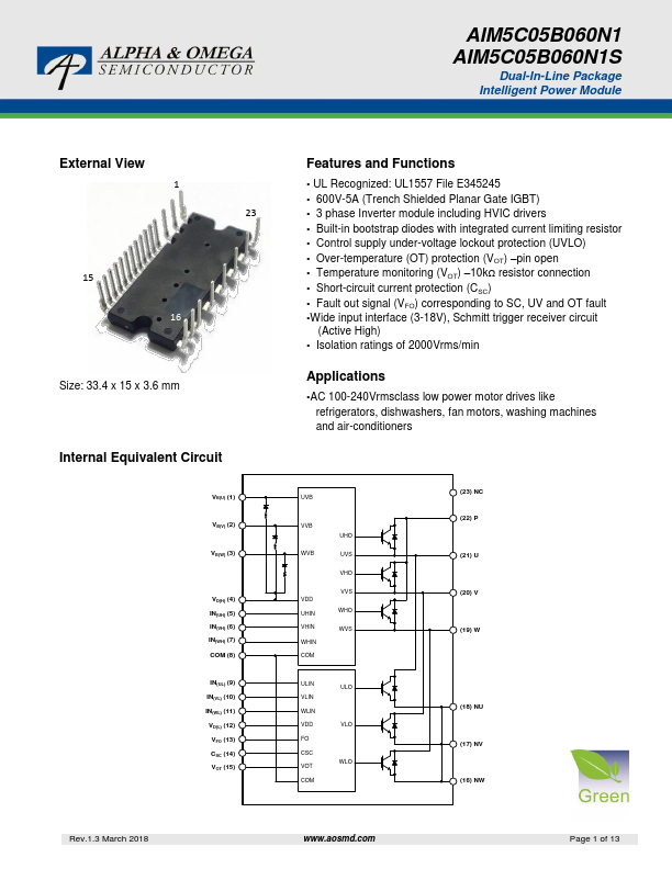
Standard pin length Short pin length Pin Description Part Number 1 2 3 4 5 6 7 8 9 10 11 12 13 14 15 16 17 18 19 20 21 22 23 Pin Name VB(U) VB(V) VB(W) VD(H) IN(UH) IN(VH) IN(WH) IN(UL) IN(VL) IN(WL) VD(L) VFO CSC VOT NW NV NU W V U P NC Pin Function High-Side Bias Voltage for U-Phase IGBT Driving High-Side Bias Voltage for V-Phase IGBT Driving High-Side Bias Voltage for W-Phase IGBT Driving High-Side mon Bias Voltage for IC and IGBTs Driving Signal Input for High-Side U-Phase Signal Input for High-Side V-Phase Signal Input for High-Side W-Phase mon Supply Ground Signal Input for Low-Side U-Phase Signal Input for Low-Side V-Phase Signal Input for Low-Side W-Phase Low-Side mon Bias Voltage for IC and IGBTs Driving Fault Output Capacitor (Low-Pass Filter) for Short-circuit Current Detection Input Over-Temperature Output Negative DC-Link Input for W-Phase Negative DC-Link Input for V-Phase Negative DC-Link Input for U-Phase Output for W-Phase Output for V-Phase Output for U-Phase Positive DC-Link Input No Connection Rev.1.3 March 2018 .aosmd. Page 2 of 13 AIM5C05B060N1 / AIM5C05B060N1S Symbol Parameter Inverter Part VPN VPN(surge) VCES Supply voltage Supply voltage (surge) Collector-emitter voltage IC Output phase current ±IPK Output peak phasecurrent PC Collector dissipation TJ Operating junction temperature Control (Protection) Part VD Control supply voltage VDB High-side control bias voltage VIN Input voltage VFO Fault output supply voltage IFO Fault output current VSC Current sensing input voltage VOT Temperature output Total System VPN(PROT) Self protection supply voltage limit (Short-circuit protection capability) TC Module case operation temperature TSTG Storage temperature VISO Isolation voltage Conditions Applied between P-NU,NV,NW Applied between P-NU,NV,NW TC=25°C, TJ<150°C TC=100°C, TJ<150°C TC=25°C, less than 1ms pulse width TC=25°C, per 1 chip Applied between VD(H)-, VD(L)- Applied between VB(U)-U, VB(V)-V, VB(W)-W Applied between IN(UH), IN(VH), IN(WH), IN(UL), IN(VL), IN(WL)- Applied between VFO- Sink current at VFO terminal Applied between CSC - Applied between VOT- VD=13.5-16.5V, Inverter part TJ=150°C, Non-repetitive, less than 2µs Measurement point of TC is provided in Figure 1 60Hz, sinusoid.
Key Features
- UL Recognized: UL1557 File E345245
- 600V-5A (Trench Shielded Planar Gate IGBT)
- 3 phase Inverter module including HVIC drivers
- Built-in bootstrap diodes with integrated current limiting resistor
- Control supply under-voltage lockout protection (UVLO)
- Over-temperature (OT) protection (VOT) –pin open
- Temperature monitoring (VOT) –10kΩ resistor connection
- Short-circuit current protection (CSC)
- Fault out signal (VFO) corresponding to SC, UV and OT fault
- Wide input interface (3-18V), Schmitt trigger receiver circuit (Active High)