Description
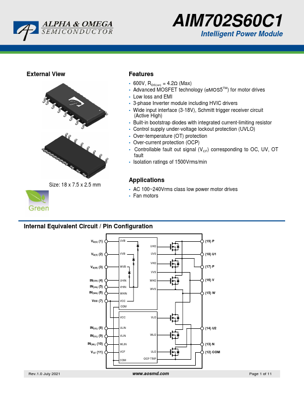
N/A P U1 P V W U2 N VB(U) VB(V) VB(W) IN(UH) IN(VH) IN(WH) Vcc IN(UL) IN(VL) IN(WL) VCF Pin Description Pin Number 1 2 3 4 5 6 7 8 9 10 11 12 13 14 15 16 17 18 19 Pin Name VB(U) VB(V) VB(W) IN(UH) IN(VH) IN(WH) VCC IN(UL) IN(VL) IN(WL) VCF N U2 W V P U1 P Rev.1.0 July 2021 Figure 1. Pin Function High-Side Bias Voltage for U-phase MOSFET Driving High-Side Bias Voltage for V-phase MOSFET Driving High-Side Bias Voltage for W-phase MOSFET Driving Signal Input for High-Side U-phase Signal Input for High-Side V-phase Signal Input for High-Side W-phase Control Supply Voltage Signal Input for Low-Side U-phase Signal Input for Low-Side V-phase Signal Input for Low-Side W-phase Controllable Fault Output mon Supply Ground Negative DC-Link Input Output for U-phase (connect to U1) Output for W-phase Output for V-phase Positive DC-Link Input Output for U-phase (connect to U2) Positive DC-Link Input .aosmd.
Key Features
- 600V, RDS(on) = 4.2Ω (Max)
- Advanced MOSFET technology (αMOS5TM) for motor drives
- Low loss and EMI
- 3-phase Inverter module including HVIC drivers
- Wide input interface (3-18V), Schmitt trigger receiver circuit (Active High)
- Built-in bootstrap diodes with integrated current-limiting resistor
- Control supply under-voltage lockout protection (UVLO)
- Over-temperature (OT) protection
- Over-current protection (OCP)
- Controllable fault out signal (VCF) corresponding to OC, UV, OT fault