EP1S40
Overview
- Chapter
- Introduction Chapter
- Stratix Architecture Chapter
- Configuration & Testing Chapter
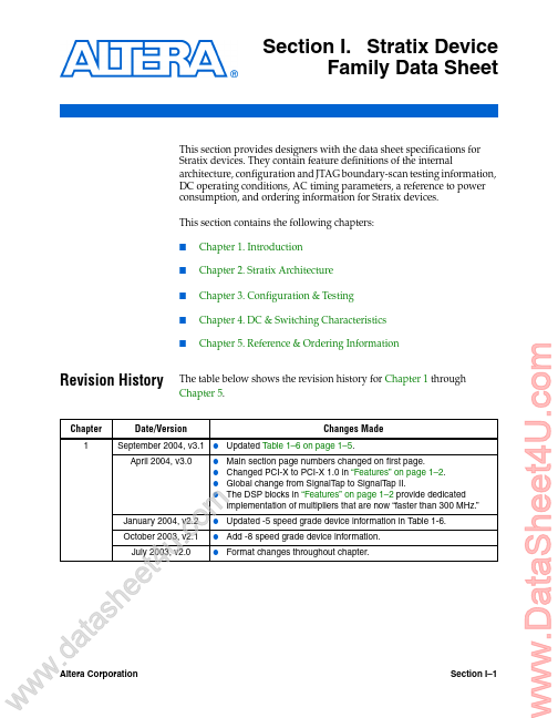
- DC & Switching Characteristics Revision History Chapter 1 The table below shows the revision history for Chapter 1 through Chapter
- Date/Version September 2004, v3.1 April 2004, v3.0 * * * *
- Changes Made Updated Table 1-6 on page 1-5. Main section page numbers changed on first page. Changed PCI-X to PCI-X 1.0 in “Features” on page 1-2. Global change from SignalTap to SignalTap II. The DSP blocks in “Features” on page 1-2 provide dedicated implementation of multipliers that are now “faster than 300 MHz.” Updated -5 speed grade device information in Table 1-6. Add -8 speed grade device information. Format changes throughout chapter. m o c . u 4 t e e h s a t a .d w w w January 2004, v2.2 October 2003, v2.1 July 2003, v2.0 * *
- Altera Corporation Section I-1 Preliminary Chapter
- Reference & Ordering Information Stratix Device Family Data Sheet Stratix Device Handbook, Volume 1 Chapter 2 Date/Version September 2004, v3.1 * * * * * * * * * * * * * * * *
- Changes Made Updated fast regional clock networks description on page 2-71. Deleted the word preliminary from the “specification for the maximum time to relock is 100 µs” on page 2-88. Added information about differential SSTL and HSTL outputs in “External Clock Outputs” on page 2-90. Updated notes in Figure 2-55 on page 2-91. Added information about