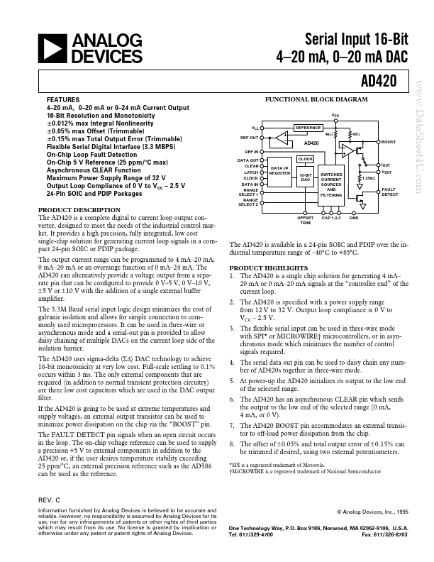
VLL REF OUT
Serial Input 16-Bit 4
20 mA, 0
20 mA DAC AD420
FUNCTIONAL BLOCK DIAGRAM
VCC REFERENCE 4kΩ 40Ω BOOST
www.DataSheet4U.com
AD420
REF IN DATA OUT CLEAR LATCH CLOCK DATA IN RANGE SELECT 1 RANGE SELECT 2 CLOCK DATA I/P REGISTER
IOUT 16-BIT DAC SWITCHED CURRENT SOURCES AND F
Key Features
4.
20 mA, 0.
20 mA or 0.
24 mA Current Output 16-Bit Resolution and Monotonicity ؎ 0.012% max Integral Nonlinearity ؎ 0.05% max Offset (Trimmable) ؎ 0.15% max Total Output Error (Trimmable) Flexible Serial Digital Interface (3.3 MBPS) On-Chip Loop Fault Detection On-Chip 5 V Reference (25 ppm/؇C max) Asynchronous CLEAR Function Maximum Power Supply Range of 32 V Output Loop Compliance of 0 V to VCC.
Full PDF Text Transcription for 420AR-32 (Reference)
Note: Below is a high-fidelity text extraction (approx. 800 characters) for
420AR-32. For precise diagrams, and layout, please refer to the original PDF.
a FEATURES 4–20 mA, 0–20 mA or 0–24 mA Current Output 16-Bit Resolution and Monotonicity ؎ 0.012% max Integral Nonlinearity ؎ 0.05% max Offset (Trimmable) ؎ 0.15% max Tot...
View more extracted text
x Integral Nonlinearity ؎ 0.05% max Offset (Trimmable) ؎ 0.15% max Total Output Error (Trimmable) Flexible Serial Digital Interface (3.3 MBPS) On-Chip Loop Fault Detection On-Chip 5 V Reference (25 ppm/؇C max) Asynchronous CLEAR Function Maximum Power Supply Range of 32 V Output Loop Compliance of 0 V to VCC – 2.5 V 24-Pin SOIC and PDIP Packages PRODUCT DESCRIPTION VLL REF OUT Serial Input 16-Bit 4–20 mA, 0–20 mA DAC AD420 FUNCTIONAL BLOCK DIAGRAM VCC REFERENCE 4kΩ 40Ω BOOST www.DataSheet4U.com AD420 REF IN DATA OUT CLEAR LATCH CLOCK DATA IN RANGE SELECT 1 RANGE SELECT 2 CLOCK DATA I/P REGISTER IOUT 16-BIT DAC SWITCHED CUR