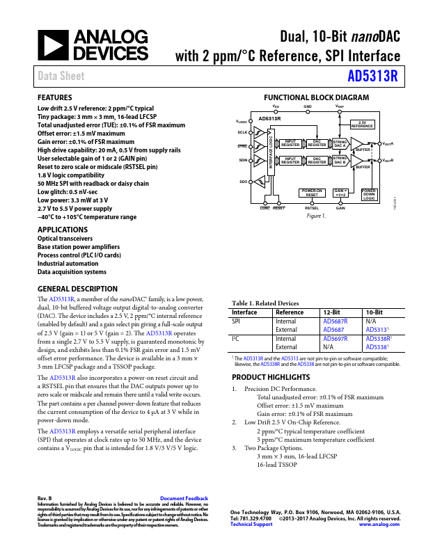
AD5313R
AD5313R is Dual 10-Bit nanoDAC manufactured by Analog Devices.
Data Sheet
Dual, 10-Bit nano DAC with 2 ppm/°C Reference, SPI Interface
Features
Low drift 2.5 V reference: 2 ppm/°C typical Tiny package: 3 mm × 3 mm, 16-lead LFCSP Total unadjusted error (TUE): ±0.1% of FSR maximum Offset error: ±1.5 m V maximum Gain error: ±0.1% of FSR maximum High drive capability: 20 m A, 0.5 V from supply rails User selectable gain of 1 or 2 (GAIN pin) Reset to zero scale or midscale (RSTSEL pin) 1.8 V logic patibility 50 MHz SPI with readback or daisy chain Low glitch: 0.5 n V-sec Low power: 3.3 m W at 3 V 2.7 V to 5.5 V power supply
- 40°C to +105°C temperature range
APPLICATIONS
Optical transceivers Base station power amplifiers Process control (PLC I/O cards) Industrial automation Data acquisition systems
GENERAL DESCRIPTION
The AD5313R, a member of the nano DAC® family, is a low power, dual, 10-bit buffered voltage output digital-to-analog converter (DAC). The device includes a 2.5 V, 2 ppm/°C internal reference (enabled by default) and a gain select pin giving a full-scale output of 2.5 V (gain = 1) or 5 V (gain = 2). The AD5313R operates from a single 2.7 V to 5.5 V supply, is guaranteed monotonic by design, and exhibits less than 0.1% FSR gain error and 1.5 m V offset error performance. The device is available in a 3 mm × 3 mm LFCSP package and a TSSOP package.
The AD5313R also incorporates a power-on reset circuit and a RSTSEL pin that ensures that the DAC outputs power up to zero scale or midscale and remain there until a valid write occurs. The part contains a per channel power-down feature that reduces the current consumption of the device to 4 μA at 3 V while in power-down mode.
The AD5313R employs a versatile serial peripheral interface (SPI) that operates at clock rates up to 50 MHz, and the device contains a VLOGIC pin that is intended for 1.8 V/3 V/5 V logic.
INTERFACE LOGIC
11254-001
VLOGIC SCLK SYNC SDIN
FUNCTIONAL BLOCK DIAGRAM
VREF
2.5V REFERENCE
INPUT REGISTER
DAC REGISTER
STRING DAC...