logo

ADCLK846 Datasheet, Analog Devices

ADCLK846 buffer equivalent, 6 lvds/12 cmos outputs low power clock fanout buffer.

ADCLK846 Avg. rating / M : 1.0 rating-11

datasheet Download

ADCLK846 Datasheet

Features and benefits

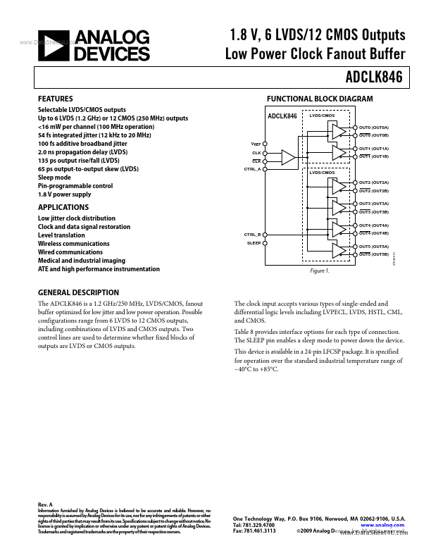
Selectable LVDS/CMOS outputs Up to 6 LVDS (1.2 GHz) or 12 CMOS (250 MHz) outputs <16 mW per channel (100 MHz operation) 54 fs integrated jitter (12 kHz to 20 MHz) 100 fs .

Application

Low jitter clock distribution Clock and data signal restoration Level translation Wireless communications Wired communic.

Description

The ADCLK846 is a 1.2 GHz/250 MHz, LVDS/CMOS, fanout buffer optimized for low jitter and low power operation. Possible configurations range from 6 LVDS to 12 CMOS outputs, including combinations of LVDS and CMOS outputs. Two control lines are used to.

Image gallery

ADCLK846 Page 1 ADCLK846 Page 2 ADCLK846 Page 3

Since 2006. D4U Semicon.   |   Contact Us   |   Privacy Policy   |   Purchase of parts