ADF4401A
ADF4401A is VCO Module manufactured by Analog Devices.
FEATURES
RF output frequency range: 62.5 MHz to 8000 MHz VCO frequency range: 4 GHz to 8 GHz 9 fs rms jitter at 8 GHz output 17 d Bm IF output power at 6 GHz RF output 90 d Bc LO_IN to RF output 90 d Bc spurious-free dynamic range Low phase noise, voltage controlled oscillator Programmable divide by 1, 2, 4, 8, 16, 32, or 64 output 3.3 V analog, digital, and mixer power supplies 5 V amplifier and VCO power supply RF output mute function 18.00 mm × 18.00 mm, 80-terminal LGA_CAV Supported in the ADIsim PLL design tool
APPLICATIONS
Instrumentation and measurement Automated test equipment Aerospace and defense
GENERAL DESCRIPTION
The ADF4401A is a fully integrated, system in package (Si P) translation loop (also known as an offset loop) module that includes a voltage controlled oscillator (VCO) and calibration phase-locked loop (PLL) circuit. Designed for highly jitter sensitive applications, this solution reduces board space and plexity pared to traditional discrete translation loop solutions designed on a printed circuit board (PCB). The time to market is significantly reduced by taking advantage of this highly integrated solution with in package circuitry and enhanced isolation that attenuates spurious ponents. The ADF4401A provides a frequency synthesis solution for engineers designing highly petitive systems.
The ADF4401A requires an external phase detector or phase frequency detector (PFD) and an external local oscillator (LO) to form a frequency synthesis solution.
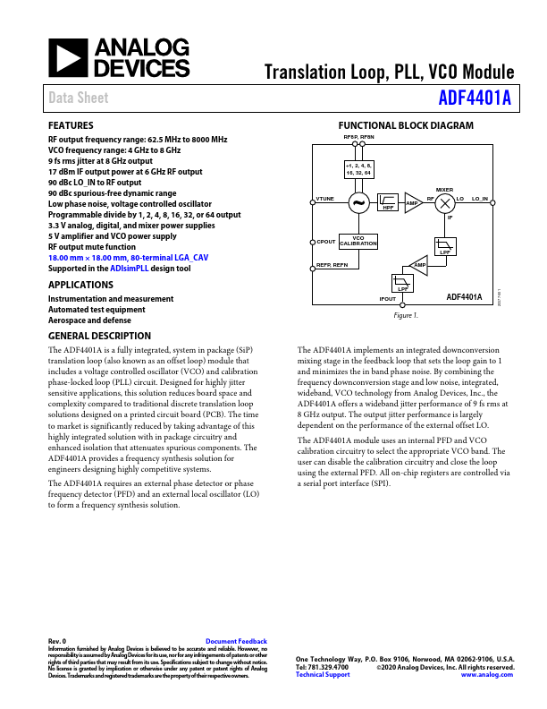
FUNCTIONAL BLOCK DIAGRAM
RF8P, RF8N
÷1, 2, 4, 8, 16, 32, 64
VTUNE
MIXER
LO LO_IN
CPOUT
VCO CALIBRATION
REFP, REFN
LPF AMP
LPF IFOUT
Figure 1.
25577-001
The ADF4401A implements an integrated downconversion mixing stage in the feedback loop that sets the loop gain to 1 and minimizes the in band phase noise. By bining the frequency downconversion stage and low noise, integrated, wideband, VCO technology from Analog Devices, Inc., the ADF4401A offers a wideband jitter...