Datasheet Summary
Data Sheet
Features
2.3 V to 5.5 V input voltage range Output voltage levels (VDDA and VDDB to VSS ≤ 35 V)
Low output voltage levels: down to
- 24.2 V High output voltage levels: up to +35 V Rise/fall time: 12 ns/19.5 ns typical Propagation delay: 80 ns typical Operating frequency: 100 kHz typical Ultralow quiescent current: 65 μA typical 20-lead, Pb-free, TSSOP package
APPLICATIONS
Low voltage to high voltage translation TFT-LCD panels Piezoelectric motor drivers
GENERAL DESCRIPTION
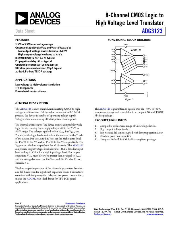
The ADG3123 is an 8-channel, noninverting CMOS to high voltage level translator. Fabricated on an enhanced LC2MOS process, the device is capable of operating at high supply voltages while maintaining ultralow...