ADM1088
FEATURES
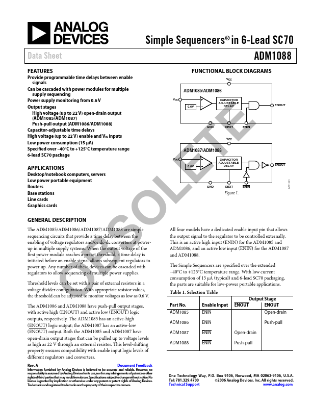
FUNCTIONAL BLOCK DIAGRAMS
Provide programmable time delays between enable
VCC signals
Can be cascaded with power modules for multiple supply sequencing
ADM1085/ADM1086
Power supply monitoring from 0.6 V Output stages
VIN 0.6V
CAPACITOR ADJUSTABLE
DELAY
ENOUT
High voltage (up to 22 V) open-drain output (ADM1085/ADM1087) Push-pull output (ADM1086/ADM1088) Capacitor-adjustable time delays High voltage (up to 22 V) enable and VIN inputs
E Low power consumption (15 μA)
Specified over
- 40°C to +125°C temperature range 6-lead SC70 package
T APPLICATIONS
Desktop/notebook puters, servers Low power portable equipment
E Routers
Base stations Line cards
L Graphics cards
GENERAL DESCRIPTION
O The ADM1085/ADM1086/ADM1087/ADM1088 are simple sequencing circuits that provide a time delay between the enabling of voltage regulators and/or dc-dc converters at powerup in multiple supply systems. When the output voltage of the
S first power module reaches a preset threshold, a time...