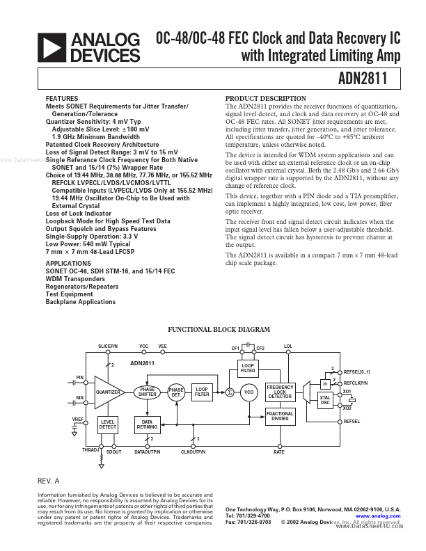
Datasheet4U Logo Datasheet4U.com

ADN2811 Datasheet - Analog Devices

OC-48/OC-48 FEC Clock and Data Recovery IC

ADN2811 Features

* Meets SONET Requirements for Jitter Transfer/ Generation/Tolerance Quantizer Sensitivity: 4 mV Typ Adjustable Slice Level: ؎ 100 mV 1.9 GHz Minimum Bandwidth Patented Clock Recovery Architecture Loss of Signal Detect Range: 3 mV to 15 mV www.DataSheet4U.com Single Reference Clock Frequency for Both

ADN2811 Datasheet (389.28 KB)

Preview of ADN2811 PDF

Datasheet Details

Part number:

ADN2811

Manufacturer:

Analog Devices ↗

File Size:

389.28 KB

Description:

Oc-48/oc-48 fec clock and data recovery ic.

📁 Related Datasheet

ADN2812 Continuous Rate 12.3 Mb/s to 2.7 Gb/s Clock and Data Recovery IC with Integrated Limiting Amp (Analog Devices)

ADN2813 Clock and Data Recovery IC (Analog Devices)

ADN2814 Continuous Rate 10 Mb/s to 675 Mb/s Clock and Data Recovery (Analog Devices)

ADN2815 Clock and Data Recovery IC (Analog Devices)

ADN2816 Continuous Rate 12.3 Mb/s to 675 Mb/s Clock and Data Recovery IC (Analog Devices)

ADN2817 (ADN2817 / ADN2818) Clock and Data Recovery IC (Analog Devices)

ADN2818 (ADN2817 / ADN2818) Clock and Data Recovery IC (Analog Devices)

ADN2819 Multirate to 2.7 Gb/s Clock and Data Recovery IC with Integrated Limiting Amp (Analog Devices)

ADN2804 Clock and Data Recovery (Analog Devices)

ADN2805 1.25 Gbps Clock and Data Recovery IC (Analog Devices)

TAGS

ADN2811 OC-48 OC-48 FEC Clock and Data Recovery Analog Devices

Image Gallery

ADN2811 Datasheet Preview Page 2 ADN2811 Datasheet Preview Page 3

ADN2811 Distributor