ADP3417
ADP3417 is Dual Bootstrapped MOSFET Driver manufactured by Analog Devices.
FEATURES
.. All-In-One Synchronous Buck Driver Bootstrapped High Side Drive One PWM Signal Generates Both Drives Anticross-Conduction Protection Circuitry APPLICATIONS Multiphase Desktop CPU Supplies Single-Supply Synchronous Buck Converters Standard-to-Synchronous Converter Adaptations
IN VCC
Dual Bootstrapped MOSFET Driver ADP3417
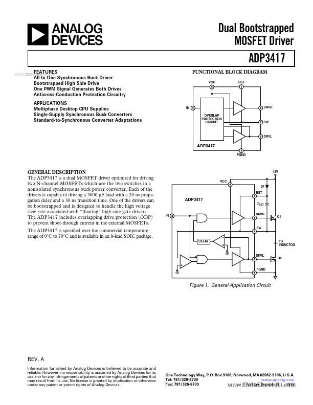
FUNCTIONAL BLOCK DIAGRAM
DRVH OVERLAP PROTECTION CIRCUIT
DRVL
PGND
GENERAL DESCRIPTION
12V VCC D1 BST
The ADP3417 is a dual MOSFET driver optimized for driving two N-channel MOSFETs which are the two switches in a nonisolated synchronous buck power converter. Each of the drivers is capable of driving a 3000 p F load with a 20 ns propagation delay and a 30 ns transition time. One of the drivers can be bootstrapped and is designed to handle the high voltage slew rate associated with “floating” high side gate drivers. The ADP3417 includes overlapping drive protection (ODP) to prevent shoot-through current in the external MOSFETs. The ADP3417 is specified over the mercial temperature range of 0°C to 70°C and is available in an 8-lead SOIC package.
CBST DRVH
Q1
DELAY
TO INDUCTOR 1V
DRVL
Q2
PGND 1V
Figure 1. General Application Circuit
REV. A
Information furnished by Analog Devices is believed to be accurate and reliable. However, no responsibility is assumed by Analog Devices for its use, nor for any infringements of patents or other rights of third parties that may result from its use. No license is granted by implication or otherwise under any patent or patent rights of Analog Devices. One Technology Way, P.O. Box 9106, Norwood, MA 02062-9106, U.S.A. Tel: 781/329-4700 .analog. Fax: 781/326-8703 © Analog Devices, Inc., 2002
ADP3417- SPECIFICATIONS1(VCC = 12 V, BST = 4 V to 26 V, T = 0؇C to 70؇C, unless otherwise noted.)
Parameter SUPPLY Supply Voltage Range Quiescent Current PWM INPUT
.. Input Voltage High2
Symbol VCC ISYS
Conditions
Min 4.15
Typ
Max 13.2 7
Unit V m A V V Ω Ω ns ns ns...