Datasheet4U Logo Datasheet4U.com

ADR821 - precision voltage reference and op amp

Download the ADR821 datasheet PDF. This datasheet also covers the ADR827 variant, as both devices belong to the same precision voltage reference and op amp family and are provided as variant models within a single manufacturer datasheet.

General Description

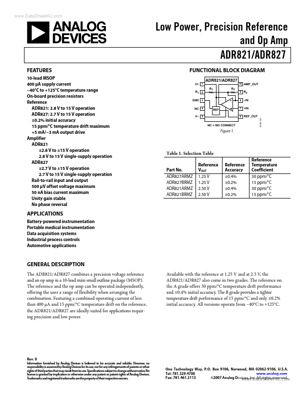
The ADR821/ADR827 combines a precision voltage reference and an op amp in a 10-lead mini small outline package (MSOP).

The reference and the op amp can be operated independently, offering the user a range of flexibility when arranging the combination.

Key Features

  • 10-lead MSOP 400 μA supply current.
  • 40°C to +125°C temperature range On-board precision resistors Reference ADR821: 2.8 V to 15 V operation ADR827: 2.7 V to 15 V operation ±0.2% initial accuracy 15 ppm/°C temperature drift maximum +5 mA/.
  • 3 mA output drive Amplifier ADR821 ±2.8 V to ±15 V operation 2.8 V to 15 V single-supply operation ADR827 ±2.7 V to ±15 V operation 2.7 V to 15 V single-supply operation Rail-to-rail input and output 500 μV offset voltage maximum 50 nA bias curre.

📥 Download Datasheet

Note: The manufacturer provides a single datasheet file (ADR827_AnalogDevices.pdf) that lists specifications for multiple related part numbers.

Full PDF Text Transcription (Reference)

The following content is an automatically extracted verbatim text from the original manufacturer datasheet and is provided for reference purposes only.

View original datasheet text
www.DataSheet4U.com Low Power, Precision Reference and Op Amp ADR821/ADR827 FEATURES 10-lead MSOP 400 μA supply current −40°C to +125°C temperature range On-board precision resistors Reference ADR821: 2.8 V to 15 V operation ADR827: 2.7 V to 15 V operation ±0.2% initial accuracy 15 ppm/°C temperature drift maximum +5 mA/−3 mA output drive Amplifier ADR821 ±2.8 V to ±15 V operation 2.8 V to 15 V single-supply operation ADR827 ±2.7 V to ±15 V operation 2.7 V to 15 V single-supply operation Rail-to-rail input and output 500 μV offset voltage maximum 50 nA bias current maximum Unity gain stable No phase reversal FUNCTIONAL BLOCK DIAGRAM V+ 1 R1 2 GND 3 NC 4 V– 5 NC = NO CONNECT REF ADR821/ADR827 R1 R2 10 AMP_OUT 9 8 7 6 R2 –IN +IN REF_OUT Figure 1. Table 1.