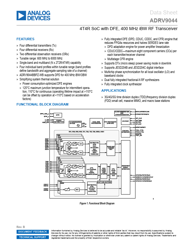
ADRV9044 Datasheet Text
Data Sheet ADRV9044
4T4R SoC with DFE, 400 MHz iBW RF Transceiver
Features
- Four differential transmitters (Tx)
- Four differential receivers (Rx)
- Two differential observation receivers (ORx)
- Tunable range: 600 MHz to 6000 MHz
- Single-band and multiband (N x 2T2R/4T4R) capability
- Four individual band profiles within tunable range (band profiles define bandwidth and aggregate sampling rate of a channel)
- ADRV9044BBPZ-WB supports DPD for 400 MHz iBW/OBW
- Simplifying system thermal solution
- Power consumption-optimized DFE engines
- 125°C maximum junction temperature for intermittent opera- tion, 110°C for continuous (operating lifetime impact at >110°C can be offset by operation at <110°C based on acceleration factors)
FUNCTIONAL BLOCK DIAGRAM
- Fully integrated DFE (DPD, CDUC, CDDC, and CFR) engine that reduces FPGAs resources and halves SERDES lane rate
- DPD adaptation engine for power amplifier linearization
- CDUC/CDDC- maximum eight ponent carriers (CCs) per each transmitter/receiver channel
- Multistage CFR engine
- Supports DTx (micro sleep) power saving mode in downlink
- Supports JESD204B and JESD204C digital interface
- Multichip phase synchronization for all local oscillator (LO) and baseband clocks
- Dual fully integrated fractional-N RF synthesizers
- Fully integrated clock synthesizer
APPLICATIONS
- 3G/4G/5G time division duplex (TDD)/frequency division duplex (FDD) small cell, massive MIMO, and macro base stations
Figure 1. Functional Block Diagram
Rev. B DOCUMENT FEEDBACK TECHNICAL SUPPORT
Information furnished by Analog Devices is believed to be accurate and reliable "as is". However, no responsibility is assumed by Analog Devices for its use, nor for any infringements of patents or other rights of third parties that may result from...