LTM8051
Quad 40VIN Silent Switcher μModule Regulator
with Configurable 1.2A Output Array
FEATURES
DESCRIPTION
n Four Complete Step-Down Switching Power Supplies
n Low Noise Silent Switcher® Architecture
n CISPR22 Class B Compliant
n CISPR25 Class 5 Compliant
n Wide Input Voltage Range: 3V to 40V
n Wide Output Voltage Range: 0.8V to 8V
n 1.2A Continuous Output Current per Channel at
12VIN, 3.3VOUT, TA = 85°C
n 1.5A Continuous Output Current per Channel at
12VIN, 3.3VOUT, TA = 60°C
n Multiphase or Multi-µModule Parallelable for
Increased Output Current
n Selectable Switching Frequency: 300kHz to 3MHz
n Compact Package (6.25mm × 11.25mm × 2.22mm)
Surface Mount BGA
APPLICATIONS
n Automated Test Equipment
n Distributed Supply Regulation
n Industrial Supplies
n Medical Equipment
All registered trademarks and trademarks are the property of their respective owners.
Click to view associated Video Design Idea.
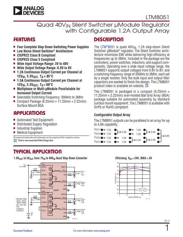
The LTM®8051 is quad 40VIN, 1.2A step-down Silent
Switcher μModule® regulator. The Silent Switcher archi-
tecture minimizes EMI while delivering high efficiency at
frequencies up to 3MHz. Included in the package are the
controllers, power switches, inductors, and support com-
ponents. Operating over a wide input voltage range, the
LTM8051 supports output voltages from 0.8V to 8V, and
a switching frequency range of 300kHz to 3MHz, each set
by a single resistor. Only the bulk input and output filter
capacitors are needed to finish the design. The LTM8051
product video is available on website.
The LTM8051 is packaged in a compact (6.25mm ×
11.25mm × 2.22mm) over-molded Ball Grid Array (BGA)
package suitable for automated assembly by standard
surface mount equipment. The LTM8051 is available with
SnPb (BGA) or RoHS compliant.
Configurable Output Array
The LTM8051 outputs can be paralleled in an array for up
to 4.8A capability.
1.2A
1.2A
2.4A
3.6A
1.2A
1.2A
4.8A
1.2A
1.2A
1.2A
TYPICAL APPLICATION
1.8-5VOUT from 7-40VIN Quad Step-Down Converter
VIN
7V to 40V
VIN1
RUN14
23.2k
RT14
fSW = 1.3MHz
SYNC14
BIAS14
VOUT1
FB1
47.5k
VOUT1
5V
47µF 1.2A
SHARE14
VCC14
VIN4
PINS NOT USED:
TRSS1, TRSS2,
TRSS3, TRSS4,
PG1, PG2, PG3,
PG4, CLKOUT14,
CLKOUT23
VIN23
RUN23
24.9k
RT23
fSW = 1.2MHz
SYNC23
SHARE23
VCC23
1µF
x4
VOUT4
FB4
GND
200k
VOUT4
1.8V
100µF 1.2A
BIAS23
VOUT2
FB2
78.7k
VOUT2
3.3V
100µF 1.2A
VOUT3
FB3
GND
118k
8051 TA01a
VOUT3
2.5V
100µF 1.2A
EEfffificcieiennccy,y,VVININ==2244VV,,BBIIAASS==55VV
95
90
85
80
75
70
65
60
3.3VOUT
5VOUT
55
0
0.5
1
1.5
2
LOAD CURRENT (A)
8051 TA01b
Document Feedback
For more information www.analog.com
Rev. 0
1