NE662M16 / 2SC5704
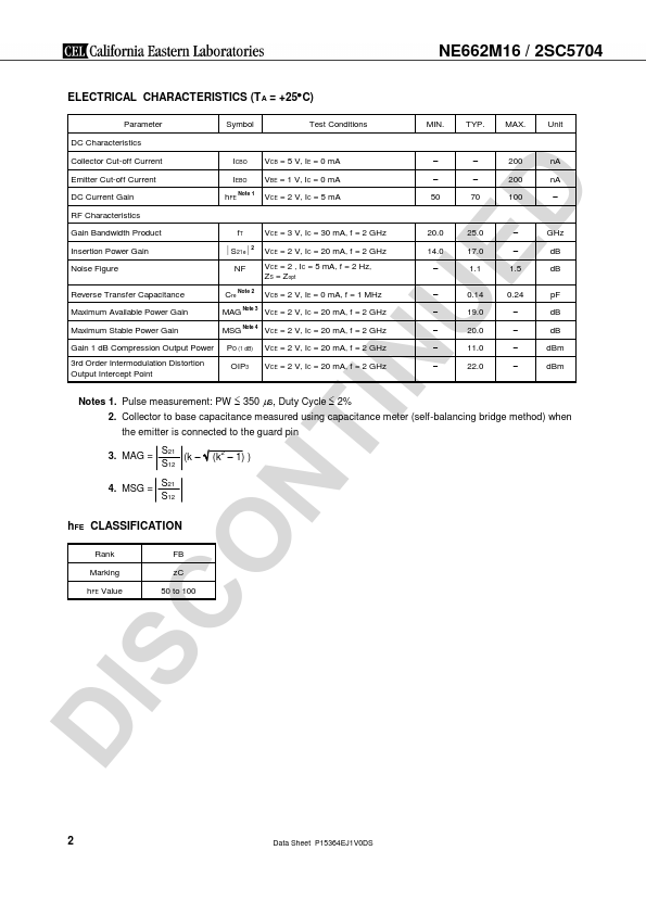
ELECTRICAL CHARACTERISTICS (TA = +25C)
Parameter
Symbol
Test Conditions
DC Characteristics
Collector Cut-off Current
ICBO VCB = 5 V, IE = 0 mA
Emitter Cut-off Current
DC Current Gain
IEBO VBE = 1 V, IC = 0 mA
hFE Note 1 VCE = 2 V, IC = 5 mA
RF Characteristics
Gain Bandwidth Product
Insertion Power Gain
Noise Figure
Reverse Transfer Capacitance
Maximum Available Power Gain
Maximum Stable Power Gain
fT VCE = 3 V, IC = 30 mA, f = 2 GHz
S21e2 VCE = 2 V, IC = 20 mA, f = 2 GHz
NF VCE = 2 , IC = 5 mA, f = 2 Hz,
ZS = Zopt
Cre Note 2 VCB = 2 V, IE = 0 mA, f = 1 MHz
MAG Note 3 VCE = 2 V, IC = 20 mA, f = 2 GHz
MSG Note 4 VCE = 2 V, IC = 20 mA, f = 2 GHz
Gain 1 dB Compression Output Power
3rd Order Intermodulation Distortion
Output Intercept Point
PO (1 dB)
OIP3
VCE = 2 V, IC = 20 mA, f = 2 GHz
MIN. TYP. MAX. Unit
– – 200 nA
– – 200 nA
50 70 100 –
20.0 25.0 – GHz
14.0 17.0
–
dB
– 1.1 1.5 dB
–
0.14 0.24
pF
19.0
dB
20.0
dB
11.0 dBm
22.0 dBm
Notes 1. Pulse measurement: PW 350 s, Duty Cycle 2%
2. Collector to base capacitance measured using capacitance meter (self-balancing bridge method) when
the emitter is connected to the guard pin
3. MAG = S21 (k – (k2 – 1) )
S12
4. MSG = S21
S12
hFE CLASSIFICATION
Rank
Marking
hFE Value
FB
zC
50 to 100
2 Data Sheet P15364EJ1V0DS