CED6861 Description
CED6861/CEU6861 P-Channel Enhancement Mode Field Effect Transistor.
CED6861 Key Features
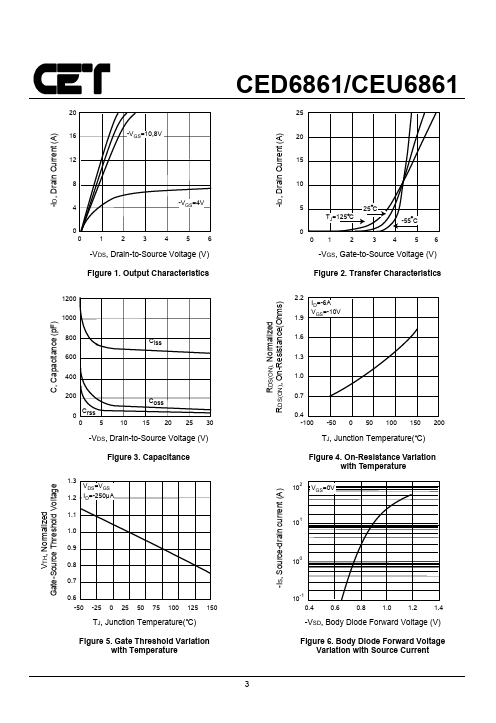
- 60V, -12A, RDS(ON) = 132mΩ @VGS = -10V. RDS(ON) = 195mΩ @VGS = -4.5V
CED6861 is P-Channel MOSFET manufactured by CET.
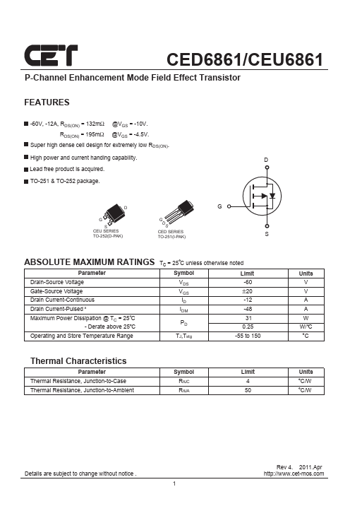
CED6861/CEU6861 P-Channel Enhancement Mode Field Effect Transistor.