Datasheet4U.com
🌙
CEM0310 Datasheet | CET
Part:
CEM0310
Description:
Single N-Channel Enhancement Mode Field Effect Transistor
Category:
Transistor
Manufacturer:
CET
Size:
691.32 KB
CEM0310 Datasheet (PDF) Download
CET
CEM0310
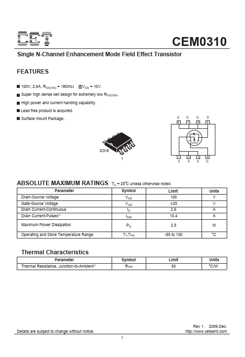
Key Features
CEM0310 Super high dense cell design for extremely low RDS(ON)
High power and current handing capability
Lead free product is acquired
Surface mount Package
×
Close