CEM3317
FEATURES
-30V, -6.2A, RDS(ON) = 33mΩ @VGS = -10V. RDS(ON) = 52mΩ @VGS = -4.5V.
-30V, -4.9A, RDS(ON) = 52mΩ @VGS = -10V. RDS(ON) = 85mΩ @VGS = -4.5V.
Super high dense cell design for extremely low RDS(ON).
High power and current handing capability.
Lead free product is acquired.
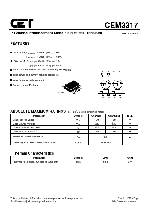
Surface mount Package.
SO-8
D1 D1 D2 D2 876 5
123 4 S1 G1 S2 G2
ABSOLUTE MAXIMUM RATINGS TA = 25 C unless otherwise noted
Parameter
Symbol
Channel 1
Drain-Source Voltage Gate-Source Voltage Drain Current-Continuous Drain Current-Pulsed a
VDS -30
VGS ±20
ID -6.2 IDM -25
Channel 2 -30
±20
-4.9 -20
Maximum Power Dissipation
PD 2.0
Operating and Store Temperature Range
TJ,Tstg
-55 to 150
Units V V A A
Thermal Characteristics
Parameter Thermal Resistance, Junction-to-Ambient b
Symbol RθJA
Limit 62.5
Units C/W
This is preliminary information on a new product in development now . Details are subject to change without notice .
Rev 1. 2006.Sep http://.cet-mos.
P-Channel(Q1)...