The following content is an automatically extracted verbatim text
from the original manufacturer datasheet and is provided for reference purposes only.
View original datasheet text
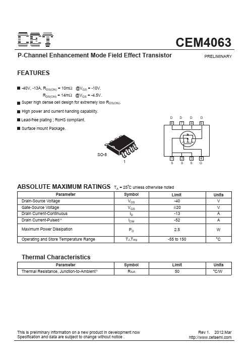
CEM4063
P-Channel Enhancement Mode Field Effect Transistor
PRELIMINARY
FEATURES
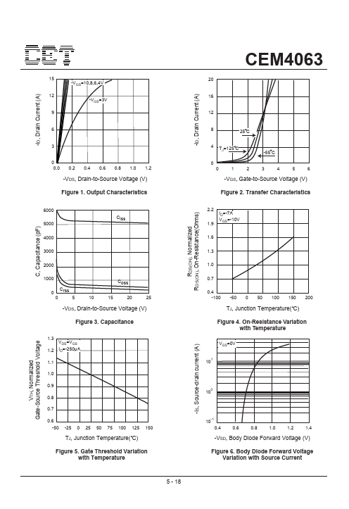
-40V, -13A, RDS(ON) = 10mΩ @VGS = -10V. RDS(ON) = 14mΩ @VGS = -4.5V.
Super high dense cell design for extremely low RDS(ON). High power and current handing capability. Lead-free plating ; RoHS compliant. Surface mount Package.
DD D D 8 7 65
SO-8
1
1 234 S SSG
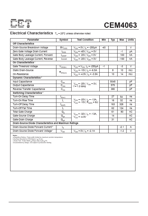
ABSOLUTE MAXIMUM RATINGS TA = 25 C unless otherwise noted
Parameter
Symbol
Limit
Drain-Source Voltage Gate-Source Voltage
VDS -40
VGS ±20
Drain Current-Continuous Drain Current-Pulsed a
ID -13 IDM -52
Maximum Power Dissipation
PD 2.
 CEM4063 Datasheet