CSD16401Q5
Features
- Ultra Low Qg & Qgd
- Low Thermal Resistance
- Avalanche Rated
- Pb Free Terminal Plating
S1 S2 S3 G4
8D 7D 6D 5D
- Ro HS pliant
- Halogen Free
QFN 5mm x 6mm Plastic Package
Top View
Product Summary
VDS Qg Qgd
RDS(on)
Vth
25 21 5.2 VGS=4.5V VGS=10V 1.5
1.8 1.3
V n C n C mΩ mΩ V
Maximum Values (TA=25o C unless otherwise stated)
Symbol
Parameter
VDS Drain to Source Voltage
VGS Gate to Source Voltage
ID Continuous Drain Current, TC = 25°C
Continuous Drain Current1
IDM Pulsed Drain Current, TA = 25°C2
PD Power Dissipation1
TJ, TSTG
Operating Junction and Storage Temperature Range
EAS Avalanche Energy, single pulse ID =100A, L = 0.1m H, RG = 25Ω
1. Rθja = 400C/W on 1in2 Cu (2 oz.) on 0.060” thick FR4 PCB. 2. Pulse width ≤300 µs, duty cycle ≤ 2%
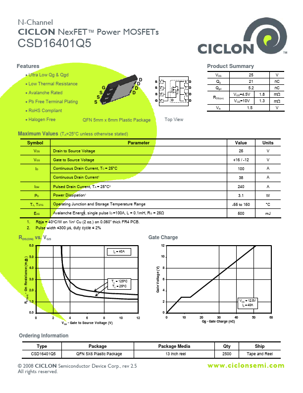
RDS(ON) vs. VGS
ID = 40A
Gate...